Wafer inspection method of charging wafer with a charged particle beam then measuring electric properties thereof, and inspection device based thereon

a technology of charged particle beam and inspection method, which is applied in the direction of individual semiconductor device testing, semiconductor/solid-state device testing/measurement, instruments, etc., can solve the problems of inaccurate measurement, difficult measurement, and unrealistic approach, and achieve the effect of changing the charge voltag

Inactive Publication Date: 2005-02-08
HITACHI LTD
View PDF6 Cites 12 Cited by
  • Summary
  • Abstract
  • Description
  • Claims
  • Application Information

AI Technical Summary

Problems solved by technology

However, with the growing trend toward finer patterns, the area to be measured tends to be as small as or smaller than the W probe, which makes measurement very difficult.
However, this approach is not realistic because the point is very soft and may deform upon contact with the object or sample.
In addition, there are three other problems.
The first problem is that if the probe and the sample are made of different materials, particularly at least one of them is a semiconductor, a Schottky junction may occur and a voltage-dependent electric resistance may be generated, which causes incorrect measurements.
Secondly, this approach is not suitable for the whole wafer surface because of its slow measuring speed.
Thirdly, because the probe touches the sample, the wafer may be contaminated such that the approach is not suitable for an in-line inspection.
Although this inspection method is speedy and suitable for whole wafer surface inspection, a brightness difference between voltage contrast images only suggests a difference in electric resistance and no quantitative data is obtained from this inspection.
In addition, depending on the orientation of a PN junction, the junction part, when electrically charged, may have a high resistance, such that it is difficult to determine whether or not there is an incomplete contact defect.
Although this inspection method is speedy and suitable for whole wafer surface inspection, whether each of the voltage contrast image portions is bright or dark merely suggests whether the resistance is high or low, and the relationship between image brightness and resistance is not indicated quantitatively such that resistance values cannot be calculated.
Therefore, it is impossible to confirm, for example, whether the reverse bias resistance value of a PN junction is correct or not.
Also this prior art claims that the positively or negatively charged wafer condition can be used to identify the orientation of a PN junction; however, if a highly electrically charged condition is produced by electron beam irradiation, the junction might break down with a resulting drastic drop in resistance.
The prior art can not identify the orientation of a PN junction which makes the inspection impossible.
According to this prior art, this problem is unavoidable because the charged voltage cannot be measured.
Besides, although electric resistances can be calculated by measuring leak currents, it takes time to make such an inspection such that the measurement cannot be made quickly.
However, this method focuses on inspection under a positively charged condition and no reference is made to inspection under a negatively charged condition.
Therefore, it is impossible to calculate the resistance-voltage characteristics of an electronic device such that it is difficult to identify the type of defect.
Another problem is that since the charged voltage cannot be controlled and measured, a breakdown of a PN junction cannot be avoided.
On the other hand, the method which uses a nano-prober has the following problems.
A second problem is that in some kind of sample, an electric resistance cannot be estimated accurately due to the contact resistance between the probe and the sample.
Another problem is that a long inspection time is required and that the whole wafer surface inspection is impossible.
However, in both methods, an inspection is made at a specific charged voltage level such that a breakdown may occur due to a high electrostatic with a resultant decline in defect detection sensitivity.
Also it is impossible to calculate the electric characteristics (resistance-voltage) of an electronic device and to identify the type of defect.
In another method in which resistance values are calculated by measuring leak currents, an inspection is made under a specific charged voltage condition and it takes time to make such an inspection; in other words, an inspection cannot be made quickly and the whole surface of a wafer can hardly be inspected.

Method used


Image

  • Wafer inspection method of charging wafer with a charged particle beam then measuring electric properties thereof, and inspection device based thereon
  • Wafer inspection method of charging wafer with a charged particle beam then measuring electric properties thereof, and inspection device based thereon
  • Wafer inspection method of charging wafer with a charged particle beam then measuring electric properties thereof, and inspection device based thereon

Examples


embodiment 1

[0050

[0051]This embodiment refers to a method by which the resistance-voltage characteristics of a sample are quickly measured in a non-contact manner so as to identify the types of defects. FIG. 7 shows a cross section of the wafer used here. It consists of a Si substrate 701, a SiO2 film 702, via (or contact) holes with an embedded poly-silicon plug 703, n-diffusion layers 704 beneath the via (or contact) holes, and PN junctions 706 formed by the diffusion layers 704. It also has an incomplete contact defect 705.

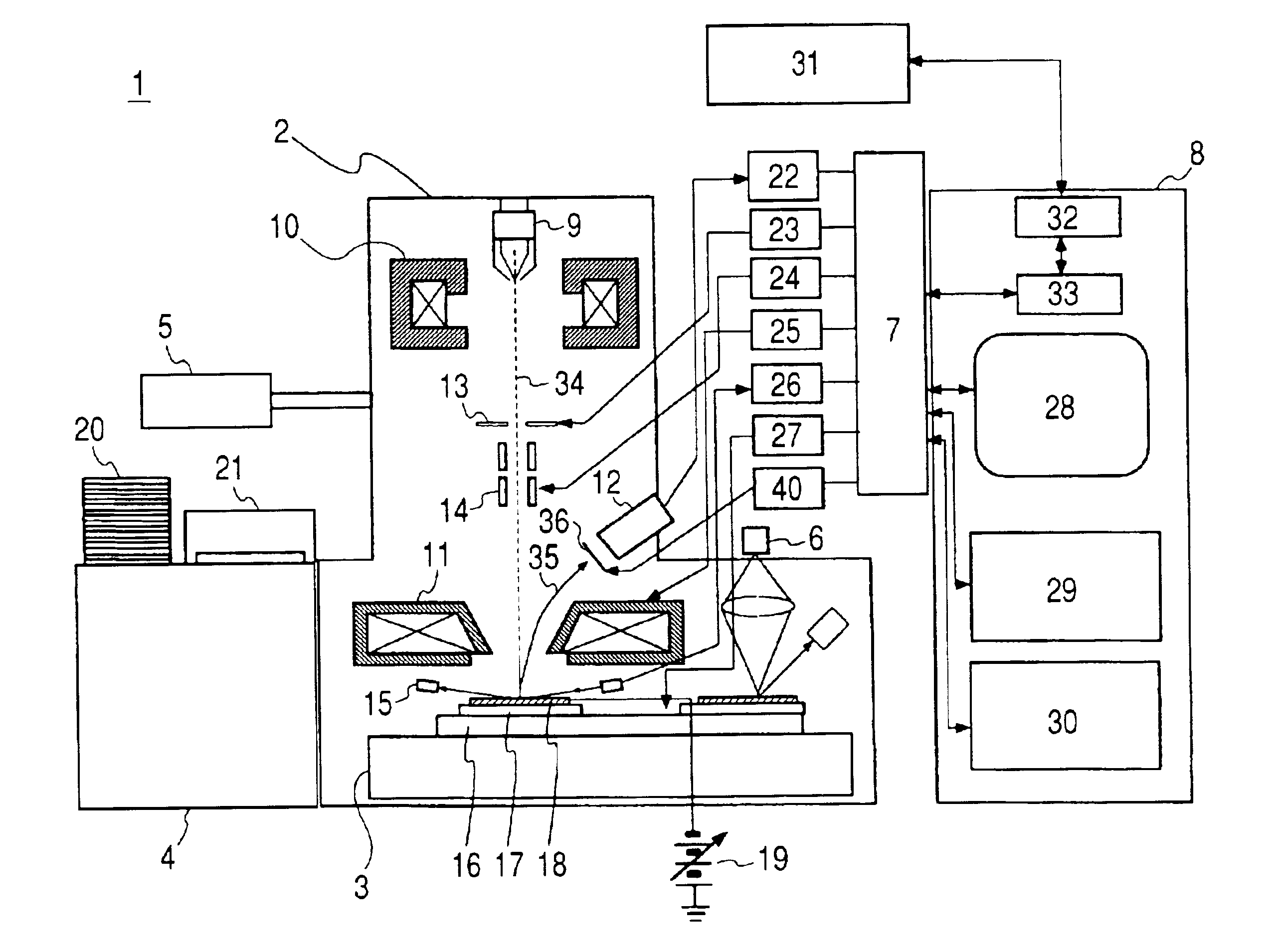
[0052]FIG. 1 shows the structure of a semiconductor device inspection device according to this embodiment. The semiconductor device inspection device 1 is mainly composed of an electron optics system 2 (i.e., an inspection chamber), a stage mechanism 3, a wafer transportation system 4, an evacuation system 5, an optical microscope 6, a control system 7 and a control section 8.

[0053]The electron optics system 2 consists of an electron gun 9 for emitting an electron beam 34,...

embodiment 2

[0071

[0072]According to the second embodiment, the resistance of each electronic device at a desired charged voltage is measured using the inspection device according to the first embodiment. If the measured resistance value is different from a predetermined value, the part in question is regarded as a defect, and the position of that defective part is displayed. The charged voltage control is performed as follows. The information on the charged voltage measured using the energy filter 36 is sent to the computing section 29 where the electron beam irradiation conditions for attaining the desired charged voltage are determined. This information is sent to the control system 7. If the desired charged voltage is not attained due to a failure in properly setting electron beam irradiation conditions, the same procedure is repeated. A detailed description of the inspection device is omitted here as the device is detailed in the explanation of the first embodiment.

[0073]This procedure can ...

embodiment 3

[0074

[0075]According to the third embodiment, we conducted an inspection of PN junctions of a CMOS formed on a wafer using the inspection device according to the first embodiment. By measuring the resistance-voltage characteristics, we could identify the orientation of PN junctions, incomplete contact defects, and leakage defects. The inspection results are shown in FIG. 12. Here, numeral 1201 designates a PN junction in which the wafer surface is an n-diffusion layer. Numeral 1202 designates a PN junction in which the wafer surface is a p-diffusion layer. Numeral 1203 designates an incomplete contact defect, and numeral 1204 designates a leakage defect. Furthermore, when inspection conditions which do not cause a breakdown are maintained by controlling the charged voltage, a judgment of inspection results can be made simply by checking variations in voltage contrast image signals (NVC and PVC). The results are shown in FIG. 13.


PUM

PropertyMeasurementUnit
charged voltagesaaaaaaaaaa

Abstract

A semiconductor defect inspection device and method for detecting defects of partially finished substrates (semiconductor wafers) for semiconductor devices is provided. The substrate surface is irradiated with a charged particle beam and a voltage contrast image is obtained while the charged voltage is controlled at a desired level, and the electric resistances of the irradiated area from the image are calculated to detect a defect and identify the type of defect. Further, the distribution of electric resistances on the whole surface of the substrate can be quickly worked out. The charged particle beam irradiation conditions are varied in order to bring the charged voltage of the area to a desired value. With this device / method, electric resistances of small portions at desired charged voltages and the corresponding electric resistances are measured in a non-contact manner to determine the type of defect. When this inspection method is applied to the PCB manufacturing process, defects can be detected and remedied at an early stage of the process. Consequently, in the semiconductor devices and other PCB related devices, the defect rate decreases and the productivity increase. Since the defect occurrence rate is reduced, the reliability of semiconductor devices is increased, and the efficiency in developing new products is improved.

Description

FIELD OF THE INVENTION[0002]The present invention relates to a device for evaluating or inspecting faults of small electronic devices formed on a wafer, and particularly to an inspection method which uses a charged particle beam to make an evaluate or inspect faults of a desired part or the whole surface of an unfinished wafer during a semiconductor device manufacturing process, and an inspection device based thereon.BACKGROUND OF THE INVENTION[0003]A semiconductor device is manufactured by repeating the process of transferring a pattern to a wafer with a photo mask by lithographic and etching techniques. Between the manufacturing stages, ion implantation takes place to form PN junctions. The processing quality in the various steps of the semiconductor device manufacturing process, including a lithographic processing step, an etching step and an ion implantation step, considerably influences the semiconductor device yield rate. Therefore, in order to improve the yield rate, it is im...

Claims


Application Information

Patent Timeline
Patent Type & Authority Patents(United States)
IPC IPC(8): G01R31/28G01R31/305G01R1/06G01R31/302G21K5/04H01J37/28H01L21/66
CPCG01R31/305
Inventor NISHIYAMA, HIDETOSHINOZOE, MARI
Owner HITACHI LTD
Why Eureka
Try Eureka