Thin film magnetic memory device including memory cells having a magnetic tunnel junction

a magnetic memory, thin film technology, applied in semiconductor devices, digital storage, instruments, etc., can solve the problems of degrading the operation reliability of the mram device, mtj memory cells having such characteristics are extremely susceptible to magnetic noise, and the data read speed cannot be increased, so as to reduce the amount of data write current, and improve the operation reliability

Inactive Publication Date: 2005-02-15
RENESAS ELECTRONICS CORP
View PDF13 Cites 6 Cited by
  • Summary
  • Abstract
  • Description
  • Claims
  • Application Information

AI Technical Summary

Benefits of technology

[0060]Therefore, a primary advantage of the present invention is that the data read speed can be increased by rapidly producing a voltage change on the first bit line by conducting the data read operation with a reduced RC constant of the data read current path, without supplying any data read current to the first read data line.
[0061]According to another aspect of the present invention, a thin film magnetic memory device having a normal operation mode and a test mode includes a memory array, a plurality of write word lines, a write word line driver, a data write circuit, and a plurality of bit line pairs. The memory array includes a plurality of magnetic memory cells arranged in rows and columns. Each of the plurality of magnetic memory cells has a different resistance value according to a level of storage data written when a data write magnetic field applied by first and second data write currents is larger than a predetermined magnetic field. The plurality of write word lines are provided corresponding to the respective rows of the magnetic memory cells, and selectively activated according a row selection result in a data write operation. The write word line driver supplies the first data write current to the activated word line in an amount corresponding to a voltage level on a first control node. The data write circuit supplies the second data write current in the data write operation in an amount corresponding to a voltage level on a second control node. The plurality of bit lines are provided corresponding to the respective columns of the magnetic memory cells, and selectively connected to the data write circuit according to a column selection result in the data write operation. At least one of the write word line driver and the data write circuit includes an input terminal for externally setting the voltage level of a corresponding one of the first and second control nodes in the test mode.
[0062]Accordingly, in the test mode, at least one of the first and second data write currents can be set from the outside. Thus, the manufacturing variation in magnetic characteristics of the MTJ memory cells can be compensated for, whereby the adjustment testing of the data write current amount for appropriately ensuring a data write margin can be facilitated.
[0063]According to a further aspect of the present invention, a thin film magnetic memory device includes a memory array, a plurality of bit lines, a plurality of write word lines, and a coupling circuit. The memory array includes a plurality of magnetic memory cells arranged in rows and columns. Each of the plurality of magnetic memory cells includes a magnetic storage portion having a different resistance value according to a level of storage data written when a data write magnetic field applied by first and second data write currents is larger than a predetermined magnetic field. The plurality of bit lines ale provided corresponding to the respective columns of the magnetic memory cells, for passing the first data write current therethrough. The plurality of write word lines are provided corresponding to the respective rows of the magnetic memory cells, and selectively activated according an address selection result so as to pass the second data write current therethrough in a data write operation. Each of the write word lines includes first and second sub write word lines respectively formed in first and second metal wiring layers with the magnetic storage portions interposed therebetween in a vertical direction on a semiconductor substrate. The coupling circuit electrically couples the first and second sub write word lines to each other. The second data write current flows as a reciprocating current through the first and second sub write word lines electrically coupled to each other by the coupling circuit.
[0064]Thus, since the data write current flows as a reciprocating current through the first and second bit lines that are electrically coupled to each other, data write magnetic fields acting in the same direction can be generated in the magnetic storage portion. This reduces the amount of data write current required to generate a data write magnetic field of the same strength. As a result, reduced power consumption of the MRAM device, improved operation reliability resulting from the reduced current density of the bit line, and also reduced magnetic field noise in the data write operation can be realized.
[0065]According to a still further aspect of the present invention, a thin film magnetic memory device includes a memory array, a plurality of read word lines, a plurality of write word lines, and a plurality of bit lines. The memory array includes a plurality of magnetic memory cells arranged in rows and columns. Each of the plurality of magnetic memory cells includes a magnetic storage portion having a different resistance value according to a level of storage data written when a data write magnetic field applied by first and second data write currents is larger than a predetermined magnetic field. The plurality of read word lines are provided corresponding to the respective rows of the magnetic memory cells, and are driven to a first voltage according to a row selection result in a data read operation. The plurality of write word lines are provided corresponding to the respective rows, and are selectively activated according an address selection result so as to pass the first data write current therethrough in a data write operation. The plurality of bit lines are provided corresponding to the respective columns of the magnetic memory cells so as to extend in such a direction that crosses the plurality of write word lines, and are each coupled to the magnetic storage portions. One of the plurality of bit lines that is selected according to an address selection result passes therethrough a data read current and the second data write current in the data read operation and the data write operation, respectively. Each of the magnetic memory cells further includes a rectifying element connected between the corresponding magnetic storage portion and the corresponding read word line.

Problems solved by technology

This voltage change cannot be quickly produced with a large RC (resistance-capacitance) time constant of the sense current path, making it impossible to increase the data read operation speed.
As a result, the MTJ memory cell having such characteristics is extremely susceptible to the magnetic noise.
Electromigration may cause disconnection or short-circuit of the wirings, thereby possibly degrading the operation reliability of the MRAM device.
Moreover, an increased data write current may possibly produce a considerable amount of magnetic noise.
As described in connection with FIGS. 87 and 88, a large number of wirings are required to write and read the data to and from the MTJ memory cell, making it difficult to reduce the area of the memory array integrating the MTJ memory cells, and thus the chip area of the MRAM device.

Method used


Image

  • Thin film magnetic memory device including memory cells having a magnetic tunnel junction
  • Thin film magnetic memory device including memory cells having a magnetic tunnel junction
  • Thin film magnetic memory device including memory cells having a magnetic tunnel junction

Examples


eighth embodiment

agram illustrating the structure of a memory array 10 and its peripheral circuitry according to a fifth modification of the

ninth embodiment

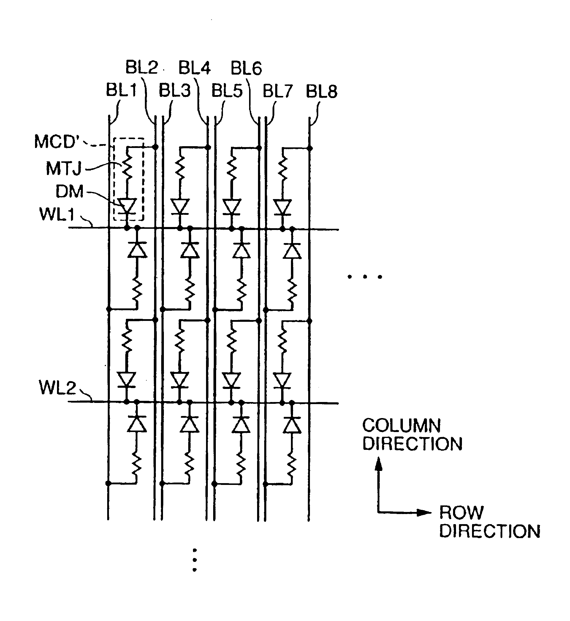
[0137]FIG. 66 is a circuit diagram showing the connection of an MTJ memory cell according to the present invention.

[0138]FIG. 67 is a timing chart illustrating the data write and read operation to and from the MTJ memory cell according to the ninth embodiment.

[0139]FIG. 68 is a structural diagram showing the MTJ memory cell arrangement according to the n ninth embodiment.

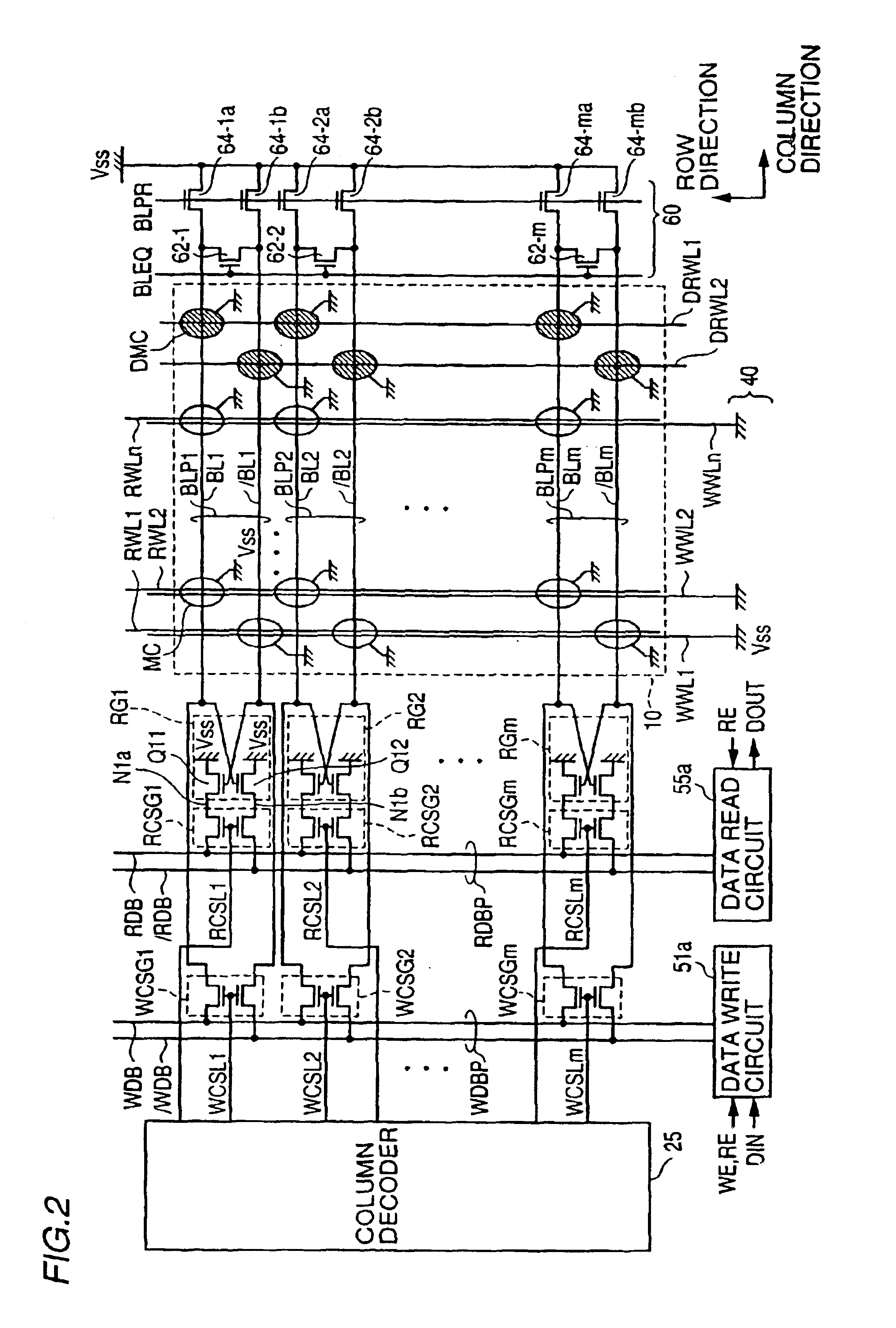
[0140]FIG. 69 is a diagram illustrating the structure of a memory array 10 and its peripheral circuitry according to the ninth embodiment.

[0141]FIG. 70 is a diagram illustrating the structure of a memory array 10 and its peripheral circuitry according to a first modification of the ninth embodiment.

[0142]FIG. 71 is a diagram illustrating the structure of a memory array 10 and its peripheral circuitry according to a second modification of the ninth embodiment.

[0143]FIG. 72 is a diagram illustrating the structure of a memory array 10 and its peripheral circuitry according to a third modification of the ninth embodimen...

tenth embodiment

[0146]FIG. 75 is a circuit diagram showing the connection of an MTJ memory cell according to the present invention.

[0147]FIG. 76 is a structural diagram showing the MTJ memory cell arrangement according to the tenth embodiment.

[0148]FIG. 77 is a diagram illustrating the structure of a memory array 10 and its peripheral circuitry according to the tenth embodiment.

[0149]FIG. 78 is a diagram illustrating the structure of a memory array 10 and its peripheral circuitry according to a first modification of the tenth embodiment.

[0150]FIG. 79 is a diagram illustrating the structure of a memory array 10 and its peripheral circuitry according to a second modification of the tenth embodiment.

[0151]FIG. 80 is a diagram illustrating the structure of a memory array 10 and its peripheral circuitry according to a third modification of the tenth embodiment.

[0152]FIG. 81 is a diagram illustrating the structure of a memory array 10 and its peripheral circuitry according to a fourth modification of the...


PUM


Abstract

In the data read operation, a memory cell and a dummy memory cell are respectively coupled to two bit lines of a selected bit line pair, and a data read current is supplied thereto. In the selected memory cell column, a read gate drives the respective voltages on a read data bus pair, according to the respective voltages on the bit lines. A data read circuit amplifies the voltage difference between the read data buses so as to output read data. The use of the read gate enables the read data buses to be disconnected from a data read current path. As a result, respective voltage changes on the bit lines are rapidly produced, whereby the data read speed can be increased.

Description

[0002]This application is a divisional of application Ser. No. 10 / 303,780 filed November 26, 2002, now U.S. Pat. No. 6,754,099, which is a continuation of application Ser. No. 10 / 066,558 filed February 6, 2002, now U.S. Pat. No. 6,501,679 which is a continuation of application Ser. No. 09 / 852,087, filed May 10, 2001, now U.S. Pat. No. 6,349,054.BACKGROUND OF THE INVENTION[0003]1. Field of the Invention[0004]The present invention relates to a thin film magnetic memory device. More particularly, the present invention relates to a random access memory (RAM) including memory cells having a magnetic tunnel junction (MTJ).[0005]2. Description of the Background Art[0006]An MRAM (Magnetic Random Access Memory) device has attracted attention as a memory device capable of non-volatile data storage with low power consumption. The MRAM device is a memory device that stores data in a non-volatile manner using a plurality of thin film magnetic elements formed in a semiconductor integrated circuit...

Claims


Application Information

Patent Timeline
Patent Type & Authority Patents(United States)
IPC IPC(8): G11C11/15G11C11/16G11C11/02G11C11/14H01L21/8246H01L27/10H01L27/105H01L43/08
CPCG11C7/12G11C7/14G11C11/16G11C11/15G11C2207/002G11C11/1653G11C11/1655G11C11/1657G11C11/1659G11C11/1673G11C11/1675G11C11/1693
Inventor HIDAKA, HIDETO
Owner RENESAS ELECTRONICS CORP
Why Eureka
Try Eureka