System and method for forming a gate dielectric

a gate dielectric and dielectric technology, applied in the field of field effect transistors, can solve the problems of slow gate area shrinkage, difficulty in maintaining gate capacitance, and difficulty in forming silicon dioxide as a dielectric gate material

Inactive Publication Date: 2005-02-22
APPLIED MATERIALS INC
View PDF145 Cites 514 Cited by
  • Summary
  • Abstract
  • Description
  • Claims
  • Application Information

AI Technical Summary

Benefits of technology

In yet another embodiment, the method of forming a dielectric stack on a semiconductor wafer comprises pre-treating the semiconductor wafer with hydrofluoric acid to form an HF-last surface, pre-treating the HF-last surface using an in-situ steam generation process, forming the dielectric stack on the pre-treated surface, and annealing the semiconductor wafer after forming the dielectric stack. The in-situ steam generation process comprises providing an inert gas flow in a process zone surrounding the HF-last surface, reacting hydrogen with an oxidizer in the process zone surrounding the HF-last surface for a very short duration, and providing an inert gas flow in the process zone after the reacting step. Preferably, the dielectric stack comprises layers of hafnium oxide, hafnium silicate layers, or a combination thereof formed using a MOCVD process.

Problems solved by technology

However, as the dimensions of the transistor continue to decrease, the continued use of silicon dioxide as a dielectric gate material is problematic.
The fundamental problem is the need to keep the capacitance of the gate high while the area of the gate is shrinking faster than the thickness of the gate dielectric.
The primary issue is that as thickness decreases, leakage current increases.
The material selected for the dielectric film affects the mobility of the carriers in the transistor channel, thereby affecting overall transistor performance.

Method used


Image

  • System and method for forming a gate dielectric
  • System and method for forming a gate dielectric
  • System and method for forming a gate dielectric

Examples


example 1

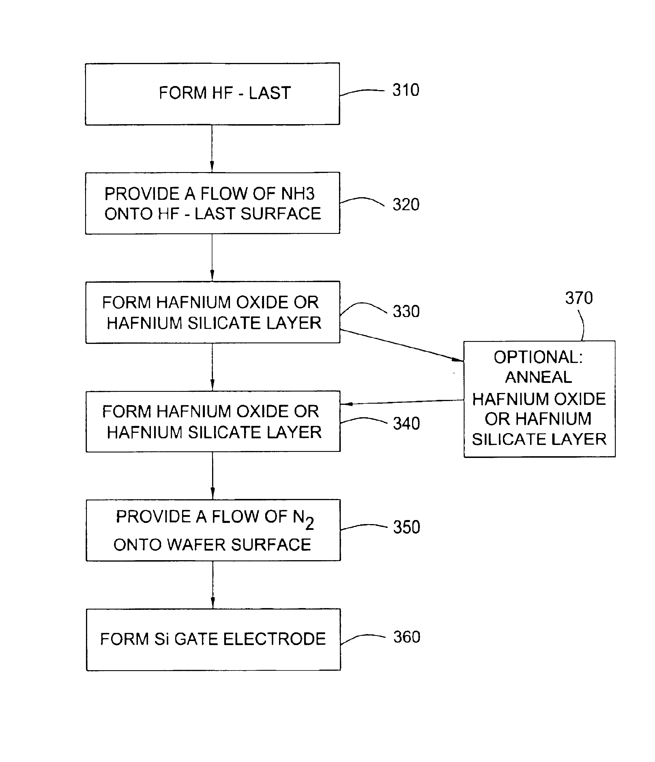
FIG. 3 illustrates the processing steps used in accordance with the invention to form a hafnium oxide, hafnium silicate, or combination thereof gate dielectric stack having an EOT of about 1.12 nanometers. At step 310, an HF-last surface is formed on a semiconductor wafer by introducing a dilute hydrofluoric acid solution onto the wafer surface for a specified time period. In one embodiment, the wafer is immersed in a hydrofluoric acid bath for a time period of about 2 minutes to about 15 minutes. More preferably, the wafer is immersed in a 2% hydrofluoric acid bath for about 2 minutes.

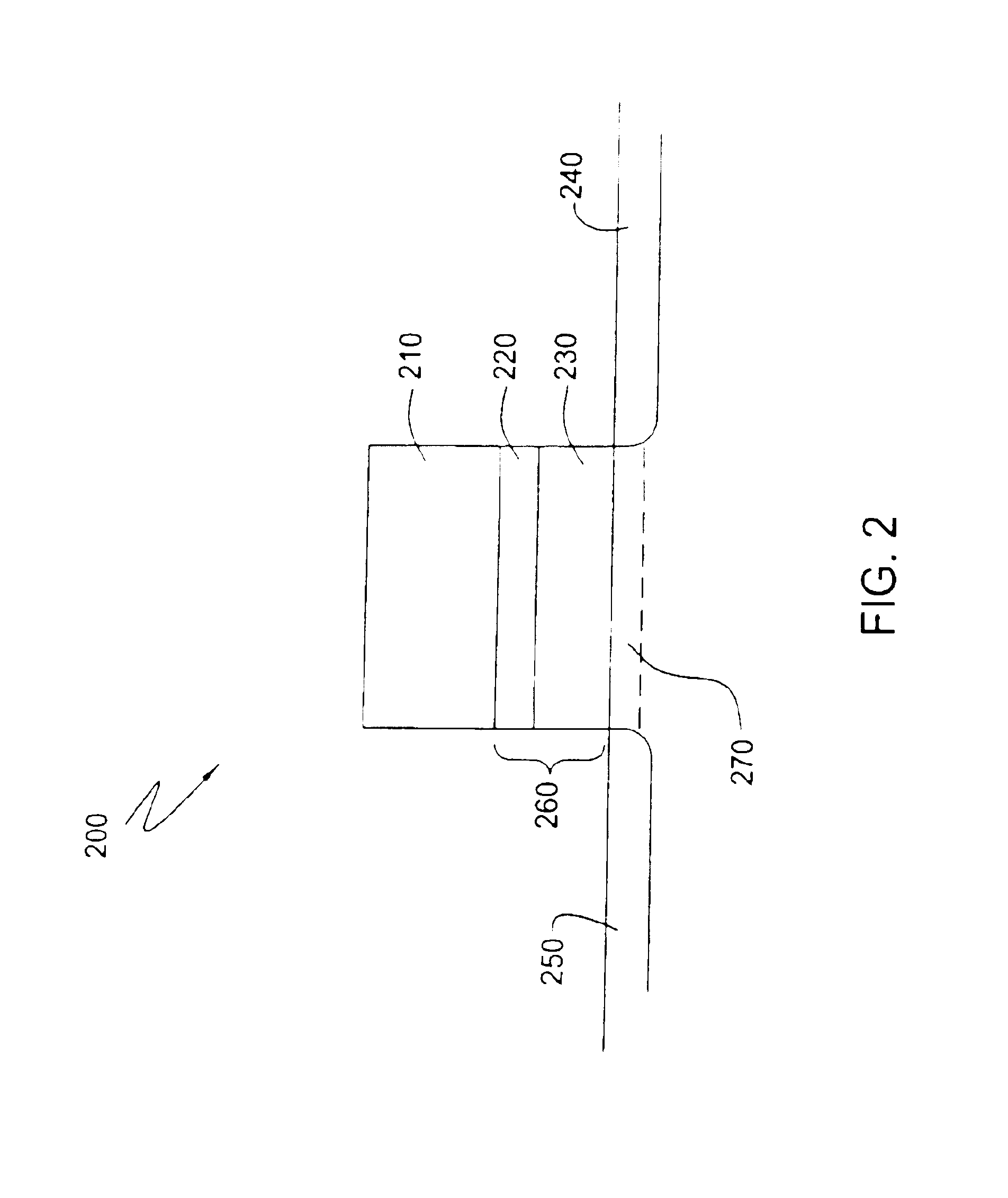
Next, the wafer is placed in a thermal chamber for pre-treating at 1 to 100 torr. A step 320, NH3 is introduced onto the HF-last surface for a specified time period and at a specified temperature. Step 320 adds a nitride “coating” or “layer” that aids in preventing the dopant of the gate layer (210 in FIG. 2) from diffusing into the channel (270 in FIG. 2). Preferably, the specified time period is in ...

example 2

FIG. 8 illustrates the processing steps used in accordance with the invention to form a hafnium oxide and hafnium silicate gate dielectric stack having a peak mobility of about 400 cm2 / Vs. At step 810, an HF-last surface is formed on a semiconductor wafer by introducing a dilute hydrofluoric acid solution onto the wafer surface for a specified time period. In one embodiment, the wafer is immersed in a hydrofluoric acid bath for a time period of about 1 minute to about 15 minutes. More preferably, the wafer is immersed in a 2% hydrofluoric acid bath for about 2 minutes.

Next, at step 820, the HF-last surface is exposed to ozonated water by, for example, immersing the wafer in an ozonated water bath. Preferably, the ozone concentration in the ozonated water is in the range of about 10 ppm to about 30 ppm. Preferably, the ozone concentration in the water is about 20 ppm. Preferably, the HF-last surface is exposed to the ozonated water for about 5 minutes to about 15 minutes. More prefer...


PUM

PropertyMeasurementUnit
temperatureaaaaaaaaaa
pressureaaaaaaaaaa
pressureaaaaaaaaaa

Abstract

A method of forming a dielectric stack on a pre-treated surface. The method comprises pre-cleaning a semiconductor wafer to remove native oxide, such as by applying hydroflouric acid to form an HF-last surface, pre-treating the HF-last surface with ozonated deionized water, forming a dielectric stack on the pre-treated surface and providing a flow of NH3 in a process zone surrounding the wafer. Alternately, the method includes pre-treating the HF-last surface with NH3, forming the stack after the pre-treating, and providing a flow of N2 in a process zone surrounding the wafer after the forming. The method also includes pre-treating the HF-last surface using an in-situ steam generation process, forming the stack on the pre-treated surface, and annealing the wafer after the forming. The pre-treating includes providing an inert gas flow in a process zone surrounding the HF-last surface, reacting hydrogen with an oxidizer in the process zone for a very short duration, and providing an inert gas flew in the process zone after the reacting.

Description

FIELD OF THE INVENTIONThe present invention relates generally to forming gate dielectric in field effect transistors, and particularly to forming metal oxide / metal silicate gate dielectric films using chemical vapor deposition.DESCRIPTION OF THE RELATED ARTThe present invention is especially useful in forming complementary metal oxide semiconductor (CMOS) integrated-circuit devices and will be described in that context. Other applications will also be mentioned. CMOS technology has enabled the microeletronic industry to simultaneously meet several technological requirements to fuel market expansion. This has been accomplished largely by a calculated reduction (scaling) of the dimensions of the field-effect transistor (FET). FIG. 1 illustrates portions of a cross sectional view of a field effect transistor (FET) pair in a typical complimentary metal oxide semiconductor (CMOS) device. Device 100 comprises a silicon wafer 155 doped with a p-type material, a p-type epitaxial silicon lay...

Claims


Application Information

Patent Timeline
Patent Type & Authority Patents(United States)
IPC IPC(8): C23C16/56C23C16/02C23C16/40H01L21/02H01L21/316
CPCC23C14/083C23C14/5806C23C14/5826C23C14/5853C23C14/586C23C16/0218C23C16/0227C23C16/405C23C16/56H01L21/28194H01L21/3141H01L21/31604H01L21/31645H01L29/517C23C14/10H01L29/78H01L21/3143H01L21/31612H01L21/3162H01L21/31683H01L21/02271H01L21/02307H01L21/02148H01L21/02181H01L21/022H01L21/02205H01L21/02337
Inventor METZNER, CRAIG R.KHER, SHREYAS S.HAN, SHIXUE
Owner APPLIED MATERIALS INC
Why Eureka
Try Eureka