

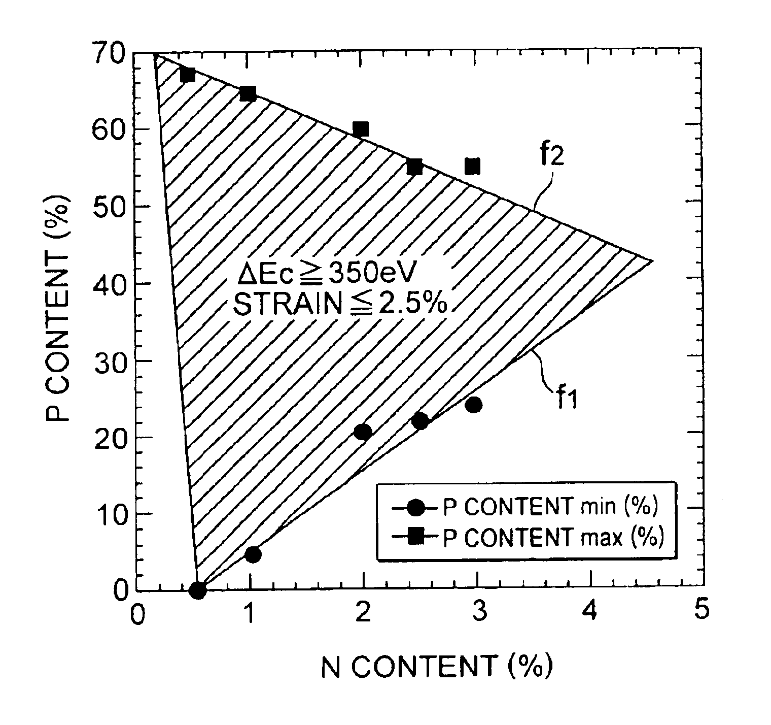
Semiconductor laser device having a high characteristic temperature
a laser device and characteristic temperature technology, applied in the direction of lasers, semiconductor devices, semiconductor lasers, etc., can solve the problems of higher current density at room temperature, cooling device for improving the characteristic temperature of the laser device cannot meet these requests, etc., to achieve the effect of reducing the threshold current density, superior crystallinity, and high characteristic temperature of the semiconductor laser devi
- Summary
- Abstract
- Description
- Claims
- Application Information
AI Technical Summary
Benefits of technology
Problems solved by technology
Method used
Image

Examples
first embodiment
Referring to FIG. 8, there is shown a 1.3-μm-band edge emitting semiconductor laser device 60 according to the present invention. The laser device 60 includes an n-GaAs substrate 62, and a layer structure formed on the (100) lattice plane of the n-GaAs substrate 62 and configured to form a resonant cavity. The layer structure includes, consecutively as viewed from the bottom, a 0.5-μm-thick n-GaAs buffer layer 64 having a carrier density of 1×1018 cm−3, a 1.5-μm-thick n-In0.48Ga0.52P cladding layer 66 having a carrier density of 1×1018 cm−3, a 0.08-μm-thick GaAs optical confinement layer 68, a GaInNAs / GaNPAs SQW active layer structure 70, 0.08-μm-thick GaAs optical confinement layer 72, a 1.5-μm-thick p-In0.48Ga0.52P cladding layer 74 having a carrier density of 1×108 cm−3, a 0.3-μm-thick p-GaAs contact layer 76 having a carrier density of 3×1019 cm−3.
The GaInNAs / GaNPAs SQW active layer structure 70 includes 8-nm-thick Ga0.63In0.37N0.01As0.99 well layer 70b, and a pair of 30-nm-thic...
second embodiment
Referring to FIG. 9, there is shown the layer structure of a 1.3-μm-band end-emitting semiconductor laser device of a ridge waveguide type according to the present invention. The semiconductor laser device 80 includes an n-GaAs substrate 82, and a layer structure formed on the (100) lattice plane of the n-GaAs substrate 82 and configured to form resonant cavity. The layer structure includes, consecutively as viewed from the bottom, a 0.5-μm-thick n-GaAs buffer layer 84 having a carrier density of 1×1018 cm−3, a 1.5-m-thick n-In0.48Ga0.52P cladding layer 86 having a carrier density of 1×1018 cm−3, a 0.08-μm-thick GaAs optical confinement layer 88, a GaInNAs / AlGaNAs SQW active layer structure 90, 0.08-μm-thick GaAs optical confinement layer 92, a 1.5-μm-thick p-In0.48Ga0.52P cladding layer 94 having a carrier density of 1018 cm−3, and a 0.3-μm-thick p-GaAs contact layer 96 having a carrier density of 3×1019 cm−3.
The GaInNAs / AlGaNAs SQW active layer structure 90 includes 8-nm-thick Ga0...
third embodiment
Referring to FIG. 10, there is shown a 1.3-μm-band surface-emitting semiconductor laser device 100 having a GaInNAsSb / GaNAsP QW active layer structure according to the present invention.
The laser device 100 includes an n-GaAs substrate 102, and a layer structure formed on the (100) lattice plane of the n-GaAs substrate 102. The layer structure includes, consecutively as viewed from the bottom, a 0.5-μm-thick n-GaAs buffer layer 104 having a carrier density of 1×1018 cm−3, a lower distributed Bragg reflector (DBR) mirror 106, a resonant cavity 108, an upper DBR mirror 110, and a p-type cap layer 118.
The lower DBR mirror 106 includes a plurality (30, in this example) of layer pairs each including an n-Al0.9GaAs layer and an n-GaAs layer. Each layer has a thickness of λ4n,
given λ being emission wavelength and given n being refractive index. The upper DBR mirror 110 includes a plurality (25, in this example) of layer pairs each including a p-Al0.9GaAs layer and a p-GaAs layer.
The λ-res...
PUM
 Abstract
Description
Claims
Application Information