Thin film transistor memory device

Inactive Publication Date: 2005-03-08
SAMSUNG ELECTRONICS CO LTD
View PDF23 Cites 20 Cited by
  • Summary
  • Abstract
  • Description
  • Claims
  • Application Information

AI Technical Summary

Benefits of technology

According to the third aspect, the memory device can have a high density without a high fabrication cost. In addition, the integrated address decoder reduces the number of connections required for the memory array to communicate with external devices, such as drivers. This feature is possible because the integrated address decoder can be coupled to each of the lines in the memory array, and may have a relatively small number of output lines connected to output devi

Problems solved by technology

Silicon wafers are expensive, raising the cost of the flash memory devices, and batch processes result in low production rates.
However, low temperature oxides are used to form the floating gate insulator in these devices.
The volatility of low temperature oxides negatively affects long-term charge storage capability.
This is undesirable because the read current may inadvertently alter t

Method used


Image

  • Thin film transistor memory device
  • Thin film transistor memory device
  • Thin film transistor memory device

Examples


Embodiment Construction

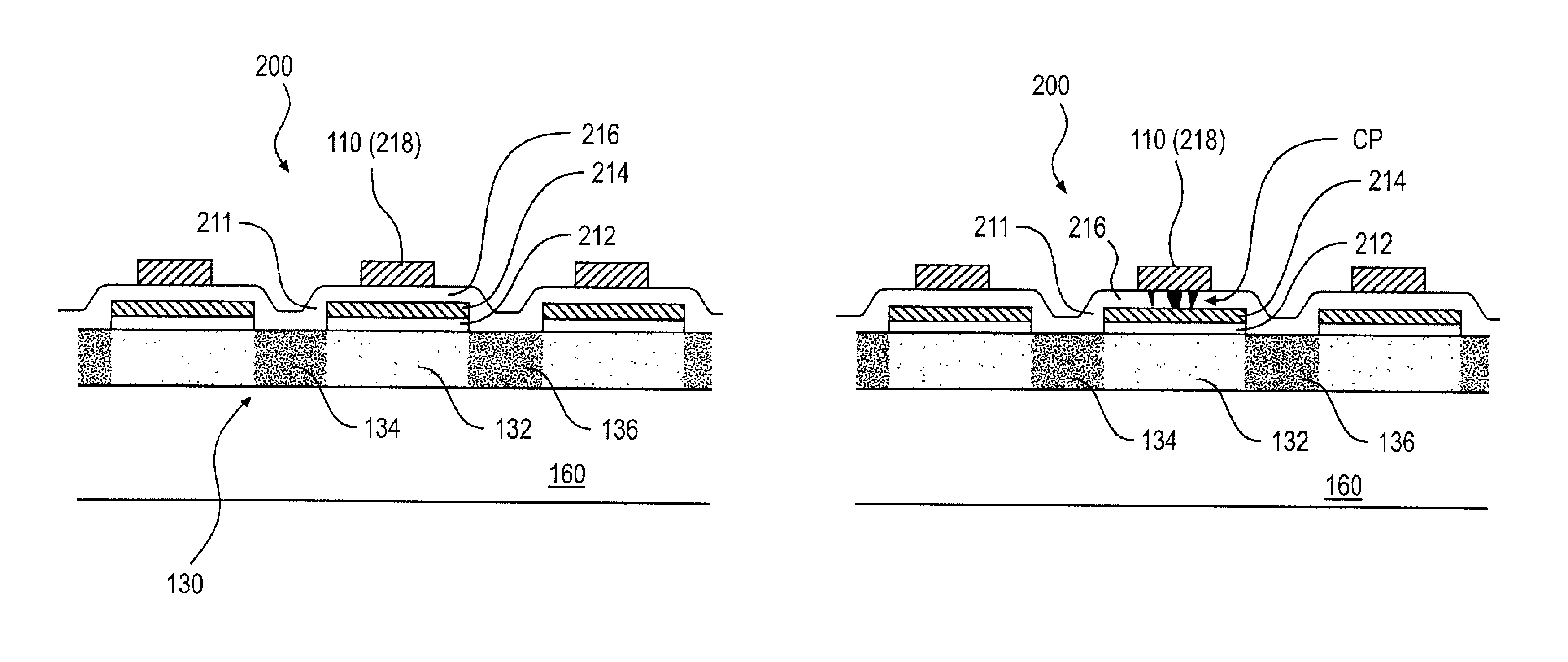
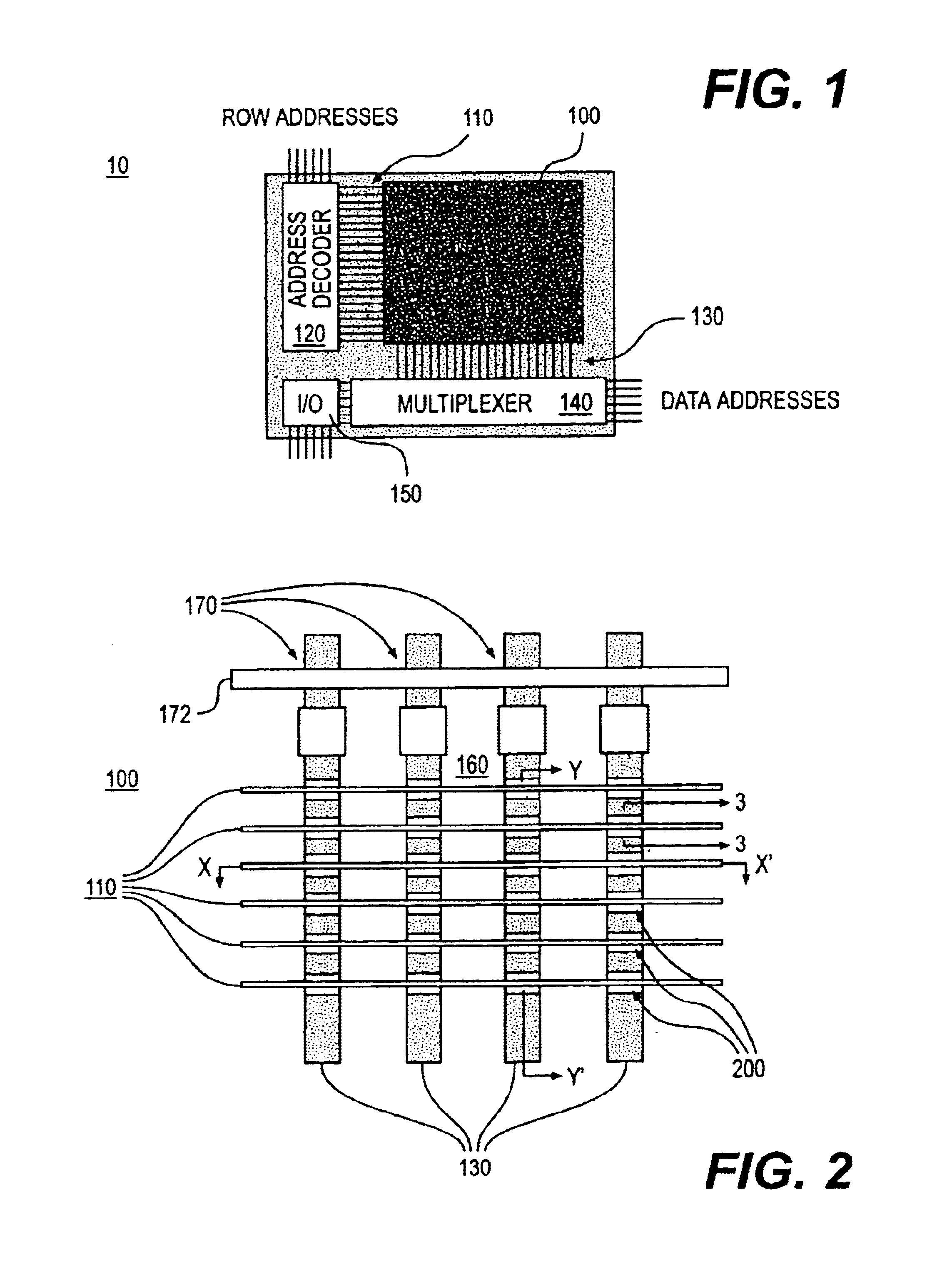
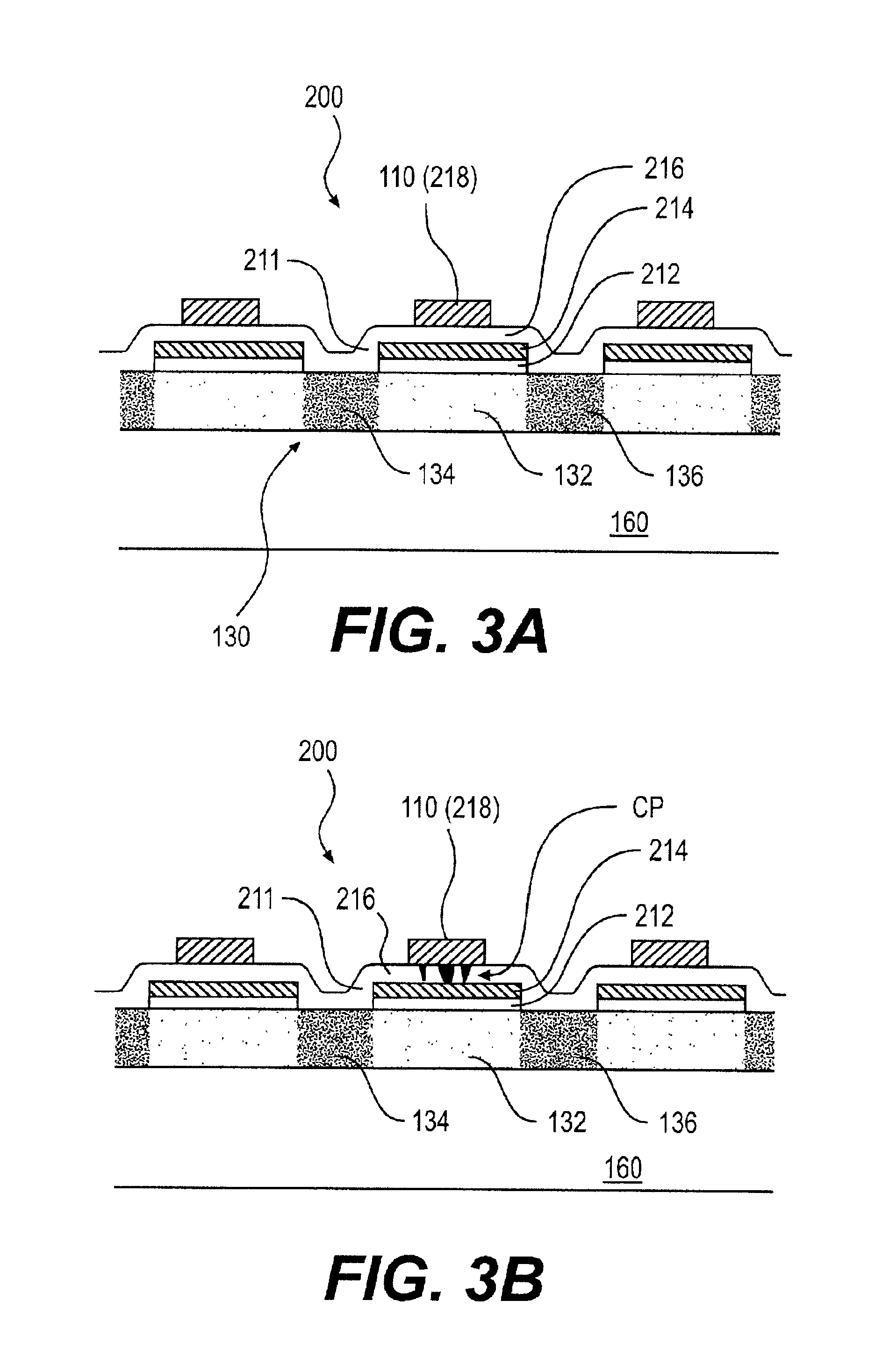
A memory device will be discussed by way of preferred embodiments and by way of the drawings.

FIG. 1 illustrates a memory device 10. The memory device 10 can be, for example, a memory card, and may be based on thin film technology. The memory device 10 includes a memory array 100 of memory cells. The memory array 100 is coupled to a row address decoder 120 and to a multiplexer 140. The multiplexer 140 is coupled to an input / output (I / O) device 150. The memory cells (not shown in FIG. 1) in the memory array 100 can be three terminal devices, such as, for example, thin film transistor (TFT) devices, and other transistor devices.

The memory array 100 stores data in the memory device 10. The address decoder 120 is coupled to gate lines 110 of the memory device 10. The address decoder 120 accesses the row of a selected memory cell 200 according to an address instruction. The multiplexer 140 is coupled to data lines 130 of the memory array 100. The multiplexer 140 combines signals from the ...


PUM


Abstract

A memory device includes a memory array of thin film transistor (TFT) memory cells. The memory cells include a floating gate separated from a gate electrode portion of a gate line by an insulator. The gate electrode portion includes a diffusive conductor that diffuses through the insulator under the application of a write voltage. The diffusive conductor forms a conductive path through the insulator that couples the gate line to the floating gate, changing the gate capacitance and therefore the state of the memory cell. The states of the memory cells are detectable as the differing current values for the memory cells. The memory cells are three terminal devices, and read currents do not pass through the conductive paths in the memory cells during read operations. This renders the memory cells robust, because read currents will not interfere with the storage mechanism in the memory cells. The memory array can be fabricated using multiple steps using the same mask. The use of a single mask for multiple steps reduces the time and cost involved in fabricating the memory array.

Description

TECHNICAL FIELDThe technical field is cross point memory arrays. More specifically, the technical field is cross point memory arrays having thin film transistor memory cells.BACKGROUNDThe growing popularity of portable electronic devices such as digital cameras and notebook computers has increased demand for inexpensive, high capacity, high performance non-volatile memory.A conventional example of a non-volatile semiconductor memory suitable for use in portable devices is flash memory. Flash memory is described in U.S. Pat. No. 4,203,158 to Frohman-Bentchkowsky et al. Flash memory utilizes an insulated floating gate to trap and retain charge over long periods of time. The states of flash memory storage elements represent binary states. Conventional flash memory devices, such as the Frohman-Bentchkowsky device, are fabricated on silicon wafers in batch processes. Silicon wafers are expensive, raising the cost of the flash memory devices, and batch processes result in low production r...

Claims


Application Information

Patent Timeline
IPC IPC(8): G11C17/14G11C17/16G11C5/06G11C16/04G11C16/02H01L21/8247H01L27/115H01L29/788H01L29/792
CPCG11C17/16G11C5/06
Inventor MEI, PINGEATON, JR., JAMES R.
Owner SAMSUNG ELECTRONICS CO LTD
Why Eureka
Try Eureka