Thermally enhanced semiconductor package with EMI shielding

a technology of shielding and semiconductors, applied in the direction of electrical equipment construction details, electrical device connections, lighting and heating apparatus, etc., can solve the problems of undetectable damage to the chip performance, heat produced by the chip is difficult to be dissipated, warpage and cracks, etc., to prevent warpage and cracks, reduce thermal stress, and ensure the structural integrity and yield of the fabricated semiconductor package

Inactive Publication Date: 2005-03-08
SILICONWARE PRECISION IND CO LTD
View PDF9 Cites 118 Cited by
  • Summary
  • Abstract
  • Description
  • Claims
  • Application Information

AI Technical Summary

Benefits of technology

The above semiconductor package yields significant benefits. The thermally conductive member is electrically coupled to the ground ring of the substrate and thus can be grounded via the substrate and solder balls, so as to provide a shielding effect for the chip and prevent the chip from being affected by external electric and magnetic interference, thereby assuring electrical performances of the chip. The thermally conductive member has a similar coefficient of thermal expansion (CTE) to that of the chip, which can reduce thermal stress induced by CTE mismatch and exerted on the chip and also prevent warpage and cracks of the chip from occurrence, such that structural integrity and yield of the fabricated semiconductor package can be assured. Moreover, the thermally conductive member is directly in contact with the chip, allowing heat produced from the chip to be effectively dissipated to the atmosphere via the thermally conductive member; as a result, the chip would not be damaged by heat accumulation or overheat, and heat dissipating efficiency of the semiconductor package can be improved. Furthermore, the thermally conductive member is simple in structure and only needs to be made in contact with the chip, thereby not increasing fabrication costs of the semiconductor package nor making fabrication processes complex to implement.

Problems solved by technology

During operation of the chip, heat is produced by consumption or conversion of electric power.
However, the chip-encapsulating resin material is relatively poor in thermal conductivity, making heat produced from the chip hard to be dissipated through the resin material to the outside, and heat accumulated in the chip would undesirably damage performances of the chip due to over heat; this overheat problem is more seriously incurred in a highly integrated chip which generates more heat in operation.
The above semiconductor package may improve heat dissipating efficiency and mechanical strength of the chip; however, it fails to provide a shielding effect for the chip, making the chip easily subject to external electric and magnetic interference (EMI) which adversely affects electrical performances of the chip.
However, in order to allow the heat spreader to be simultaneously in contact with the ground ring on the substrate and the chip and to allow a side of the heat spreader to be exposed outside, a particularly designed and complexly shaped heat spreader needs to be prepared for the above semiconductor package, which not only increases fabrication costs but also makes fabrication processes more complicated to implement.
Further, it is not easy to accurately control progress of the processes for making the complexly structured heat spreader, which may thus degrade dimensional preciseness or yield of the fabricated products; for example, if thickness or heights of the protruding portion and support portions of the heat spreader are formed with dimensional errors, the heat spreader can not properly come into contact with the chip and the ground ring of the substrate simultaneously, and thus heat dissipating and EMI shielding performances would be adversely affected for the semiconductor package.

Method used


Image

  • Thermally enhanced semiconductor package with EMI shielding
  • Thermally enhanced semiconductor package with EMI shielding
  • Thermally enhanced semiconductor package with EMI shielding

Examples


first preferred embodiment

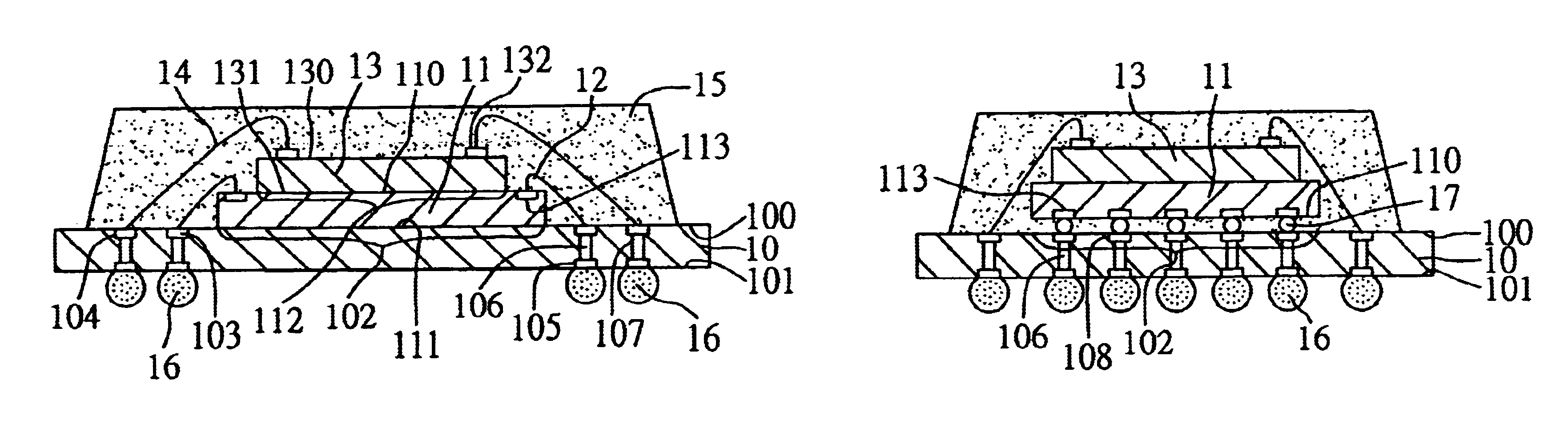
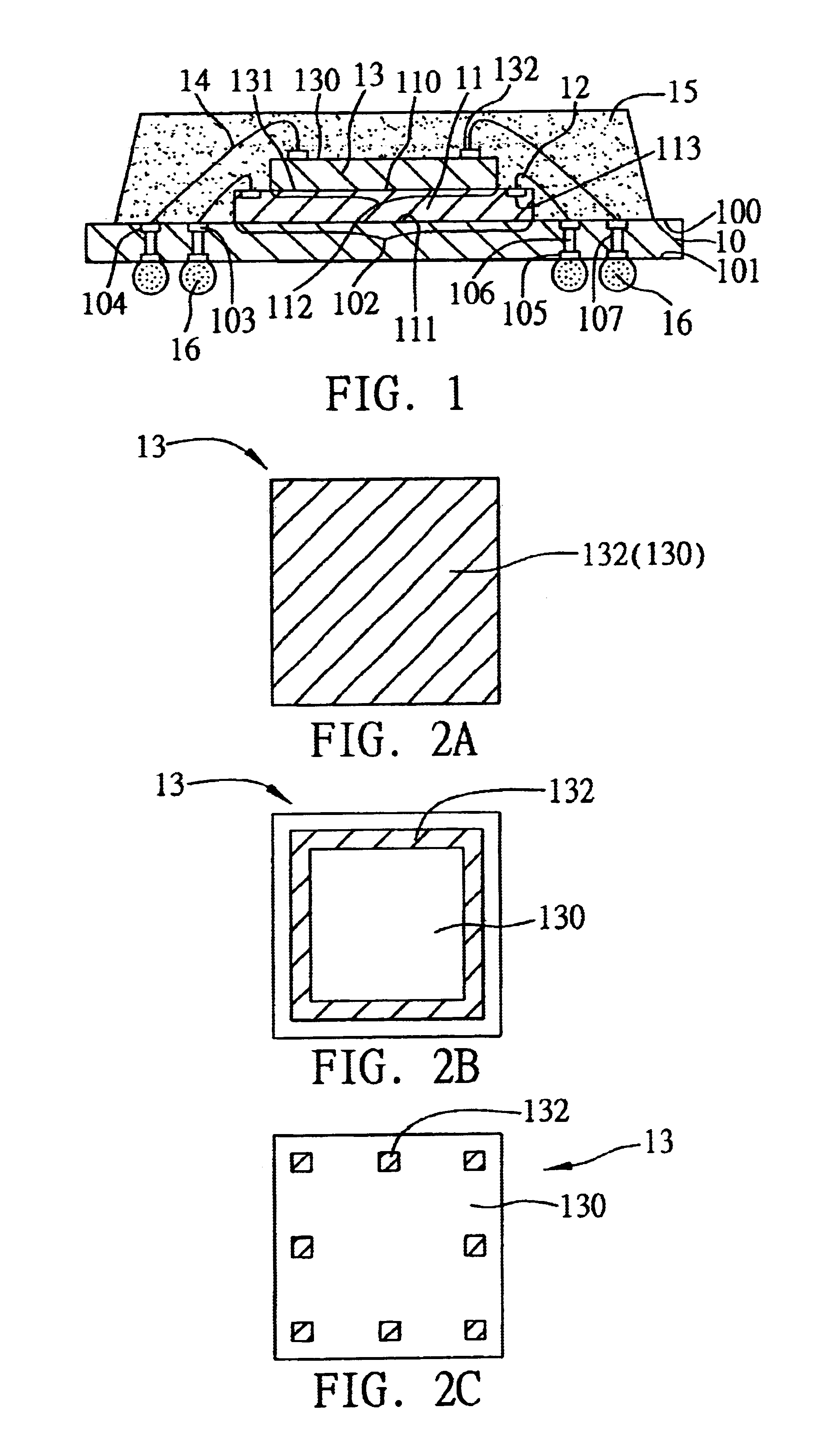
FIG. 1 illustrates a semiconductor package according to a first preferred embodiment of the invention. As shown in the drawing, this semiconductor package utilizes a substrate 10 as a chip carrier; the substrate 10 is primarily made of a conventional resin material such as epoxy resin, polyimide resin, BT (bismaleimide triazine) resin, FR4 resin, etc.

The substrate 10 has an upper surface 100 and a lower surface 101 opposed to the upper surface 100, wherein the upper surface 100 is defined with a chip attach area 102, a plurality of bond fingers 103 and a ground ring 104 surrounding the bond fingers 103 are formed outside the chip attach area 102, and a plurality of ball pads 105 are disposed on the lower surface 101 of the substrate 100. The substrate 10 is further formed with a plurality of conductive vias 106 and ground vias 107 penetrating therethrough, wherein the conductive vias 106 have one end thereof connected to the bond fingers 103 and the other end connected to the corres...

second preferred embodiment

FIG. 3 illustrates a semiconductor package according to a second preferred embodiment of the invention. This semiconductor package differs from that of the first embodiment in the way of electrical connection between the chip and substrate. As shown in FIG. 3, the active surface 110 of the chip 11 is mounted in a face-down manner on the chip attach area 102 and electrically connected to the upper surface 100 of the substrate 10 by a plurality of solder bumps 17, wherein the solder bumps 17 have one end thereof connected to a plurality of bond pads 108 formed on the chip attach area 102 and the other end connected to the bond pads 113 formed on the active surface 110 of the chip 11. Further, the conductive vias 106 formed through the substrate 10 have one end thereof connected to the bond pads 108 of the substrate 10 and the other end connected to the solder balls 16 implanted on the lower surface 101 of the substrate 10. This face-down arrangement of the chip electrically coupled to...

third preferred embodiment

FIG. 4 illustrates a semiconductor package according to a third preferred embodiment of the invention. This semiconductor package differs from that of the above second embodiment in that a surface of the thermally conductive member is exposed to outside of the chip-encapsulating encapsulant. As shown in FIG. 4, by the flip-chip arrangement of the chip 11 electrically connected to the substrate 10 via the solder bumps 17, a thermally conductive member 13 larger in surface area than the chip 11 can be used, wherein a recessed portion 133 of a step-like shape (not limited to this) is formed at peripheral area on the first surface 130 of the thermally conductive member 13, and the metal layer 132 is applied over the recessed portion 133 to be connected with bonding wires 14. The recessed portion 133 has a depth greater than a loop height of the bonding wires 14 protruding from the metal layer 132 to allow loops of the bonding wires 14 to be comfortably received with the recessed portion...


PUM


Abstract

A thermally enhanced semiconductor package with EMI (electric and magnetic interference) shielding is provided in which a chip is mounted on and electrically connected to a surface of a substrate, and a thermally conductive member is stacked on the chip and electrically coupled to the surface of the substrate by bonding wires. An encapsulant is formed and encapsulates the chip, thermally conductive member, and bonding wires. A plurality of solder balls are implanted on an opposite surface of the substrate. The thermally conductive member is grounded via the bonding wires, substrate, and solder balls, and provides an EMI shielding effect for the chip to protect the chip against external electric and magnetic interference. The thermally conductive member has a coefficient of thermal expansion similar to that of the chip, and reduces thermal stress exerted on the chip and enhances mechanical strength of the chip to thereby prevent chip cracks.

Description

FIELD OF THE INVENTIONThe present invention relates to semiconductor packages, and more particularly, to a thermally enhanced semiconductor package with EMI (electric and magnetic interference) shielding to improve electrical performances of the semiconductor package.BACKGROUND OF THE INVENTIONA semiconductor package is a structure incorporated with a chip that is made of a semiconductor material such as silicon and encapsulated or packaged with an insulating resin material such as epoxy resin, to allow delicate circuits and electronic elements formed on the chip to be protected by the resin material from external moisture and contaminant. During operation of the chip, heat is produced by consumption or conversion of electric power. However, the chip-encapsulating resin material is relatively poor in thermal conductivity, making heat produced from the chip hard to be dissipated through the resin material to the outside, and heat accumulated in the chip would undesirably damage perfo...

Claims


Application Information

Patent Timeline
Patent Type & Authority Patents(United States)
IPC IPC(8): H01L25/065H01L23/31H01L23/28H01L23/433H01L23/552H01L23/34
CPCH01L23/3128H01L23/552H01L25/0657H01L23/4334H01L2224/48227H01L2224/16225H01L2224/32145H01L2224/48225H01L2224/48247H01L2225/0651H01L2225/06517H01L2225/06541H01L2924/01079H01L2924/15311H01L2924/19107H01L2924/3025H01L24/48H01L2224/73265H01L2224/32225H01L2924/07802H01L2224/16235H01L2924/00012H01L2924/00H01L24/73H01L2224/05639H01L2224/05644H01L2224/45099H01L2224/48091H01L2224/85399H01L2924/00014H01L2924/181H01L2224/45015H01L2924/207
Inventor LIN, YING-RENTSAI, HO-YI
Owner SILICONWARE PRECISION IND CO LTD
Why Eureka
Try Eureka