Enhanced silicidation of polysilicon gate electrodes

a technology of gate electrodes and polysilicon, which is applied in the direction of semiconductor devices, semiconductor/solid-state device details, electrical equipment, etc., can solve the problems of limiting the circuit operating speed, becoming increasingly difficult to accurately form discreet devices on semiconductor substrates exhibiting the requisite reliability,

Inactive Publication Date: 2005-03-15
ADVANCED MICRO DEVICES INC
View PDF4 Cites 43 Cited by
  • Summary
  • Abstract
  • Description
  • Claims
  • Application Information

AI Technical Summary

Benefits of technology

An advantage of the present invention is a method of manufacturing a semiconductor device having relatively thick metal silicide contacts on gate electrodes and relatively thin metal silicide contacts on source/drain regions.
Another advantage of the present invention is a semiconductor device having relatively thick metal silicide contacts on gate electrodes and relatively thin metal silicide contacts on associated source/drain regions.
Additional advantages and other features of the present invention will be set forth in part in the description which follows, and in part will become apparent to those having ordinary skill in the art upon examination of the following or may be learned by practice of the present invention. The advantages of the present invention may be realized and obtained as particularly pointed out in the appended claims.
According to the present invention, the foregoing and other advantages are achieved in part by a method of manufacturing a semiconductor device, the method comprising: forming a plurality of polysilicon gate electrodes, each having an upper surface and side surfaces, over an upper surface of a silicon substrate with a gate dielectric layer therebetween; forming source/drain regions on the upper surface of the substrate on opposite sides of each gate electrode with a channel region therebetween; forming a metal silicide layer, having a first thickness, on the upper surface of the gat...

Problems solved by technology

As integrated circuit geometries continue to plunge into the deep sub-micron regime, it becomes increasingly more difficult to accurately form discreet d...

Method used


Image

  • Enhanced silicidation of polysilicon gate electrodes
  • Enhanced silicidation of polysilicon gate electrodes
  • Enhanced silicidation of polysilicon gate electrodes

Examples


Embodiment Construction

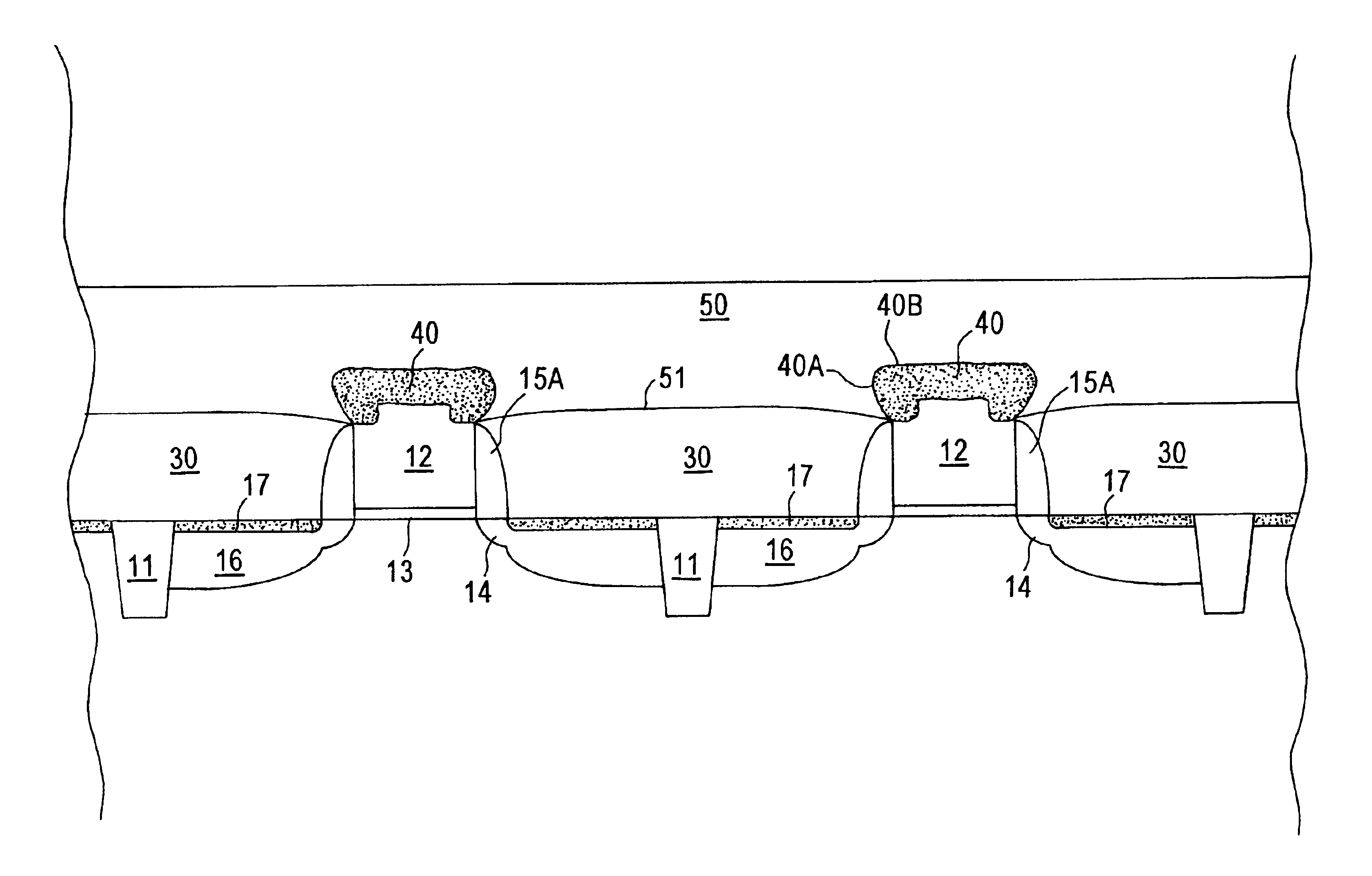
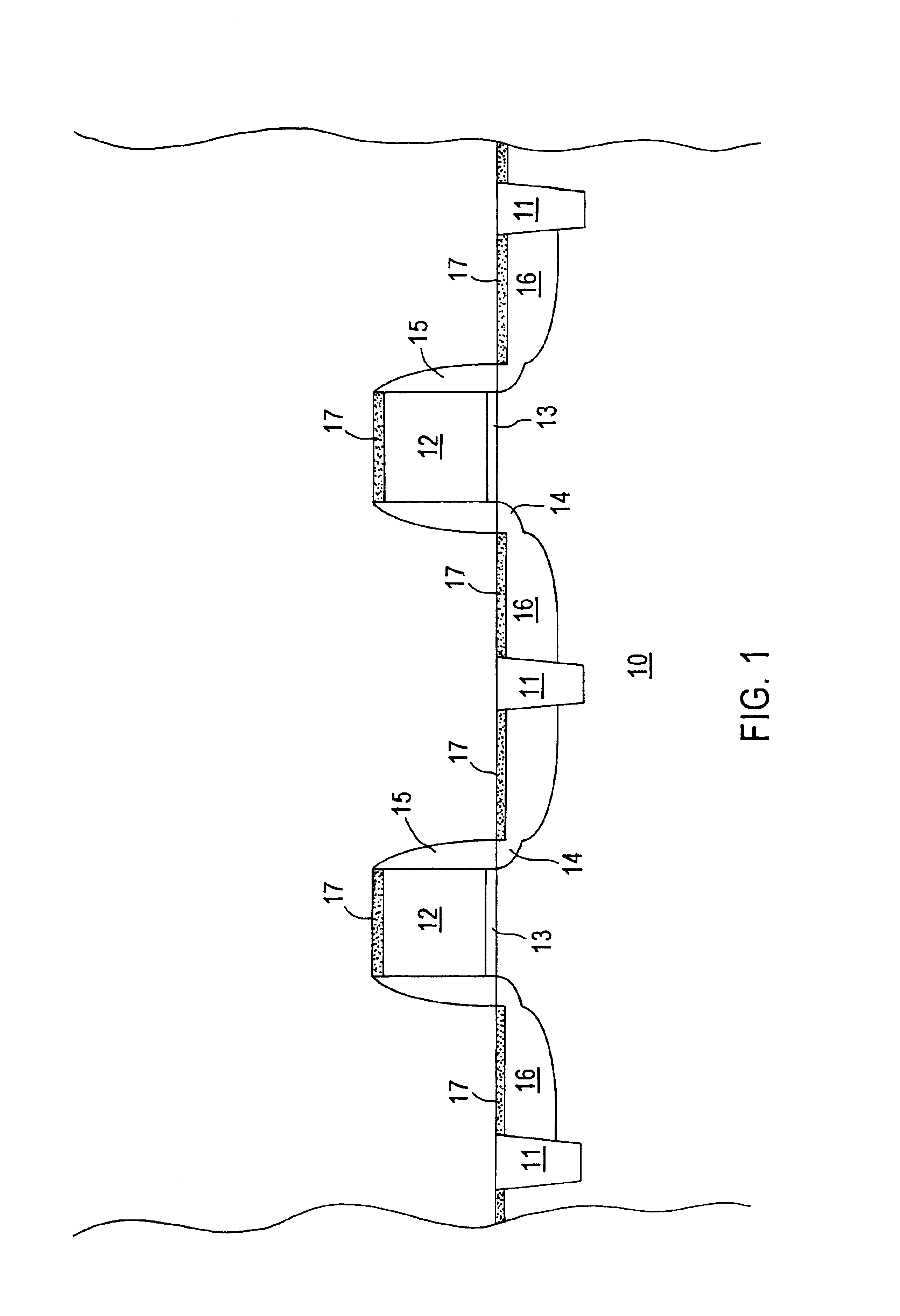
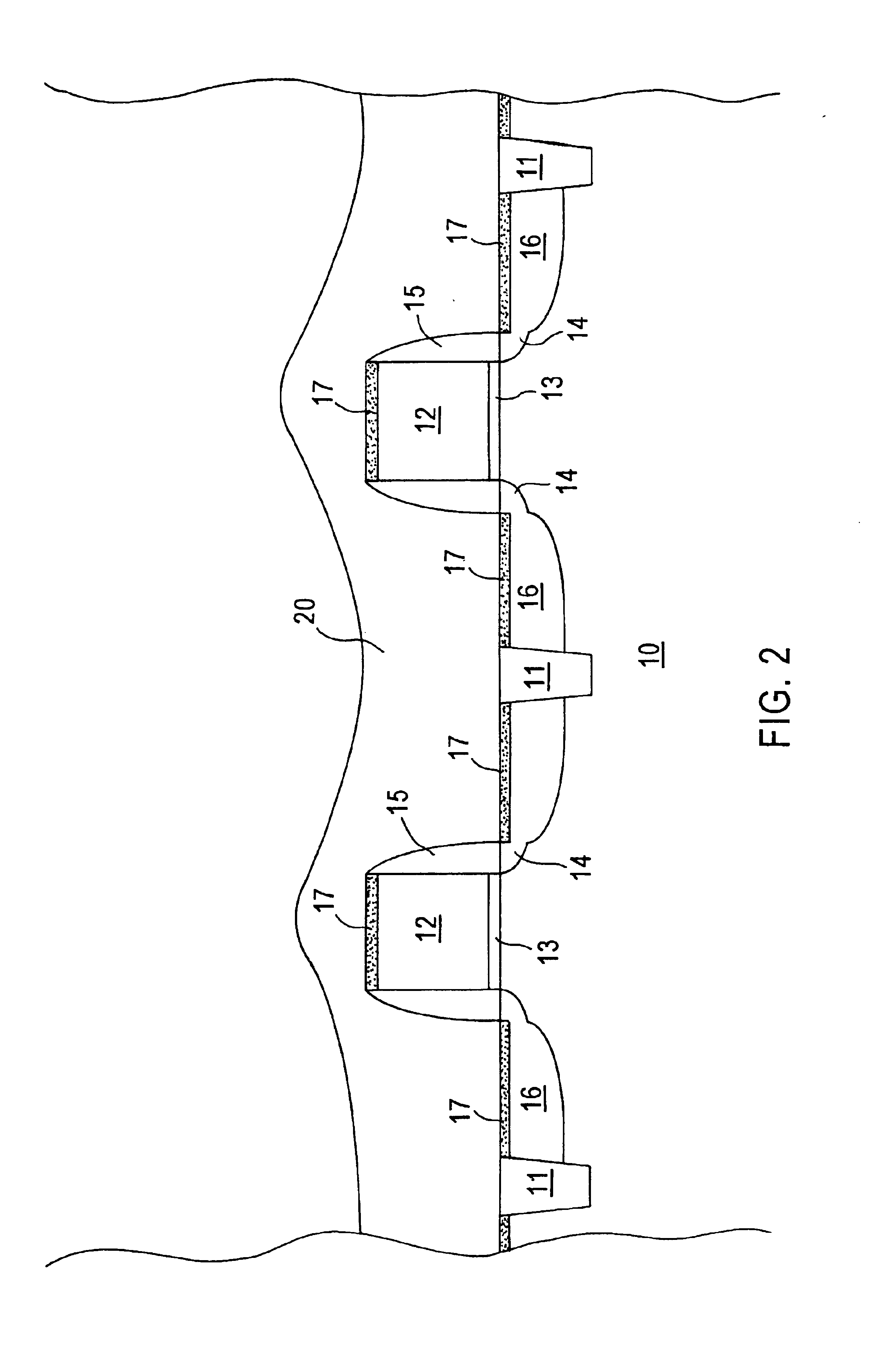
The present invention addresses and solves problems attendant upon implementing conventional salicide technology in fabricating micro-miniaturized semiconductor devices. As device geometries shrink into the deep sub-micron regime, the operating speed becomes an issue. Accordingly, it is desirable to form a relatively thick metal silicide layer on the gate electrodes. However, as the thickness of the metal silicide layers formed on the source / drain region increases and / or the junction depth decreases, metal silicide spiking occurs through the junction as well as metal silicide separation. The present invention addresses and solves that problem generated by conflicting processing objectives by providing efficient methodology enabling the fabrication of semiconductor devices having a relatively thick metal silicide layer on the gate electrodes while having a relatively thin metal silicide layer on the source / drain regions.

In accordance with embodiments of the present invention, an init...


PUM


Abstract

Semiconductor devices exhibiting reduced gate resistance and reduced silicide spiking in source/drain regions are fabricated by forming thin metal silicide layers on the gate electrode and source/drain regions and then selectively resilicidizing the gate electrodes. Embodiments include forming the thin metal silicide layers on the polysilicon gate electrodes and source/drain regions, depositing a dielectric gap filling layer, as by high density plasma deposition, etching back to selectively expose the silicidized polysilicon gate electrodes and resilicidizing the polysilicon gate electrodes to increase the thickness of the metal silicide layers thereon. Embodiments further include resilicidizing the polysilicon gate electrodes including a portion of the upper side surfaces forming mushroom shaped metal silicide layers.

Description

TECHNICAL FIELDThe present invention relates to the fabrication of micro-miniaturized, high speed semiconductor devices, particularly to self-aligned silicide (salicide) technology, and the resulting semiconductor devices. The present invention is particularly applicable to ultra large scale integrated circuit (ULSI) systems having features in the deep sub-micron regime.BACKGROUND ARTAs integrated circuit geometries continue to plunge into the deep sub-micron regime, it becomes increasingly more difficult to accurately form discreet devices on a semiconductor substrate exhibiting the requisite reliability. High performance microprocessor applications require rapid speed of semiconductor circuitry. The speed of semiconductor circuitry varies inversely with the resistance (R) and capacitance (C) of the interconnection system. The higher the value of the R×C product, the more limiting the circuit operating speed. Miniaturization requires long interconnects having small contacts and sma...

Claims


Application Information

Patent Timeline
IPC IPC(8): H01L21/4763H01L21/02H01L21/44H01L21/28H01L21/285H01L21/336H01L29/423H01L29/78
CPCH01L21/28114H01L21/28518H01L29/66507H01L29/42376H01L29/7833H01L29/6659
Inventor KARLSSON, OLOV B.CHAN, SIMON S.EN, WILLIAM G.MICHAEL, MARK W.
Owner ADVANCED MICRO DEVICES INC
Why Eureka
Try Eureka