Electro-optical device
an electrooptical device and display technology, applied in the field of electrooptical display (electroluminescence) display, can solve the problems of no concrete proposal, short life of the el element, etc., and achieve the effect of preventing flickering by the alternate curren
- Summary
- Abstract
- Description
- Claims
- Application Information
AI Technical Summary
Benefits of technology
Problems solved by technology
Method used
Image

Examples
embodiment 1
[Embodiment 1]
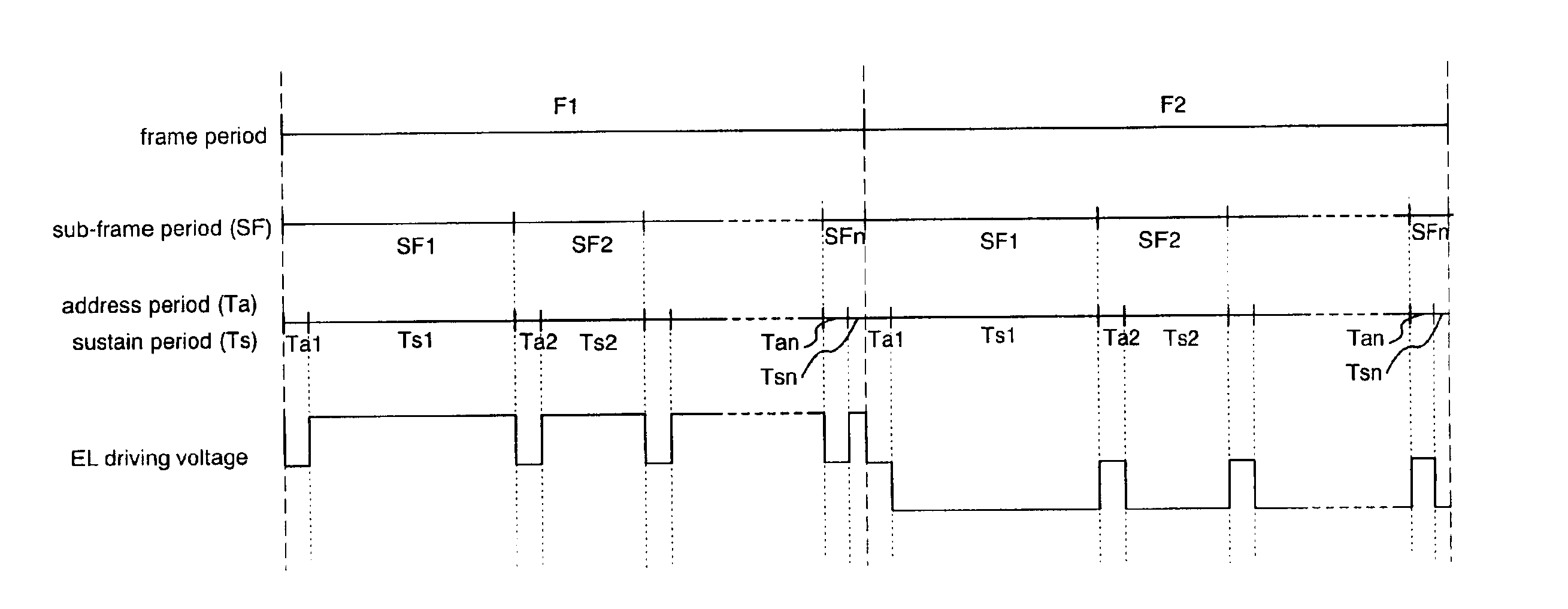
In Embodiment 1, there will be explained a case in which the polarity of the on EL driving voltage is changed to the opposite polarity for each sub-frame period in the case where the time division gray scale display is provided in the digital-style driving with the alternate current. Here, there will be explained a case in which 2n grays scale full-color time division gray scale display is provided by the n-bit digital device method.
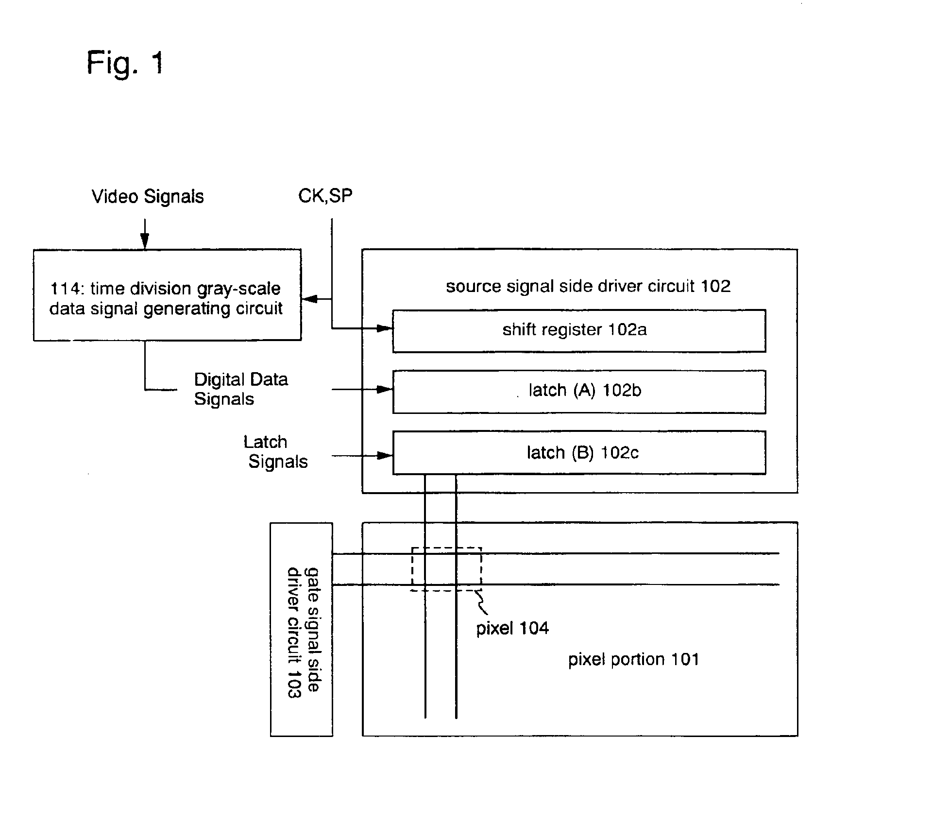
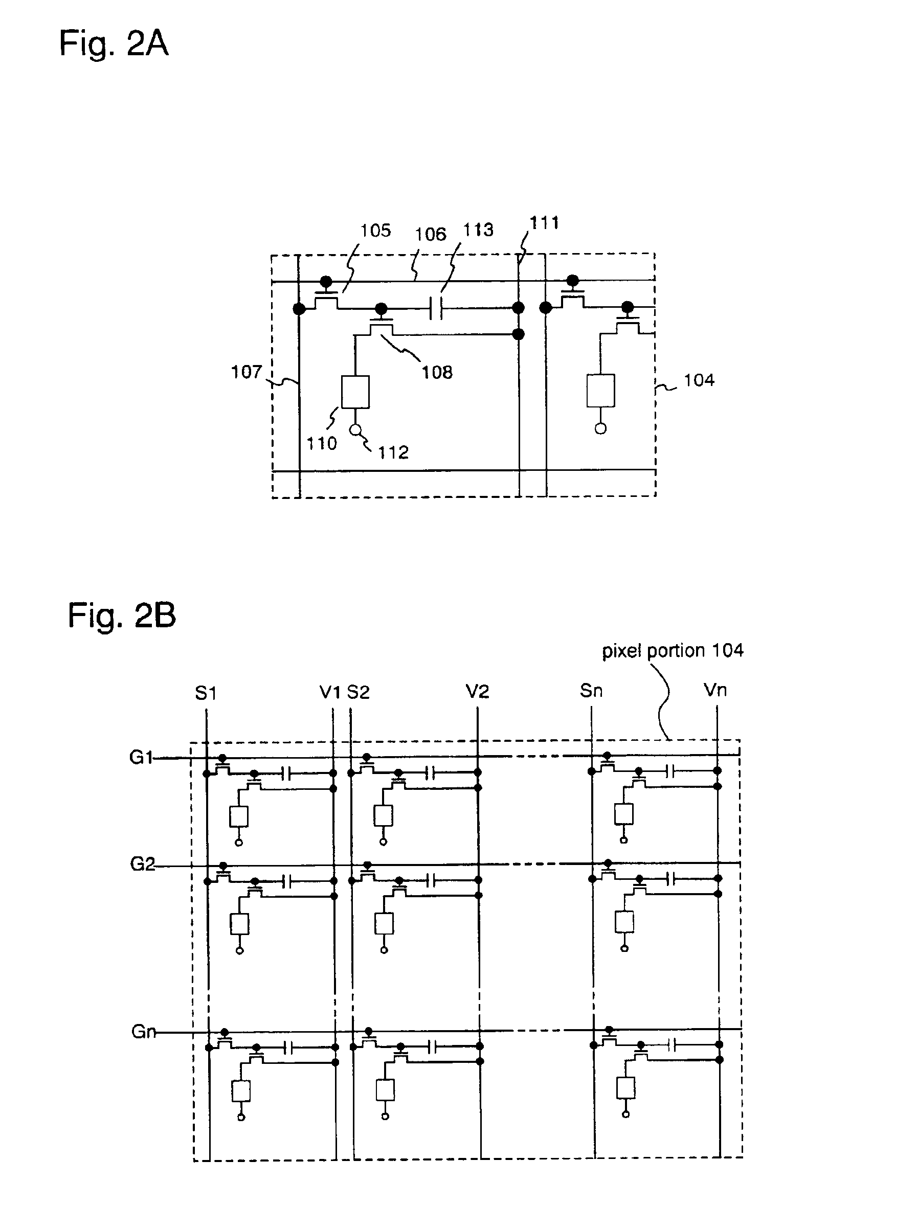
The structure of the pixel portion of the EL display in Embodiment 1 is the same as the structure shown in FIG. 2B. The gate signal lines (G1 through Gn) are connected to the gate electrode of the switching TFT incorporated in each of the pixels. One of the source region and the drain region of the switching TFTs incorporated in each of the pixels is connected to the source signal lines (S1 through Sn) while the other is connected to the gate electrode of the EL driving TFTs and the capacitor. Furthermore, one of the source region and the d...
embodiment 2
[Embodiment 2]
In Embodiment 2, an example is shown which is different from the pixel portion of the EL display according to the present invention shown in FIG. 2A.
FIG. 6A shows a circuit diagram showing an example of an enlarged view of the pixel portion of the EL display according to Embodiment 2. In the pixel portion, a plurality of pixels are arranged in a matrix-like configuration. The pixel 603 and the pixel 604 are provided adjacent to each other. In FIG. 6A, reference numerals 605 and 625 denote switching TFTs. The gate electrode of the switching TFTs 605 and the 625 are connected to the gate signal line 606 to which the gate signal is inputted. One of the source region and the drain region of switching TFTs 605 and 625 is connected to the data signal lines (also referred to as source signal lines) 607 and 627 to which the digital data signal is inputted while the other is connected to the gate electrode of the EL driving TFTs and the capacitors 613 and 633, respectively.
Then...
embodiment 3
[Embodiment 3]
Next, reference is made to FIG. 7 schematically showing the sectional structure of the EL display device of the present invention.
In FIG. 7, reference numeral 11 is a substrate, and 12 is an insulating film that is a base (hereinafter, this film is designated as base film). For the substrate 11, use can be made of a light transmissible substrate, representatively, a glass substrate, a quartz substrate, a glass ceramic substrate, or a crystallized glass substrate. However, it must be resistible to the highest processing temperature in a manufacturing process.
The base film 12 is effective especially in using a substrate that has a movable ion or a substrate that has conductivity, but it is not necessarily disposed on the quartz substrate. An insulating film that contains silicon can be used as the base film 12. It should be noted that, in this specification, “insulating film that contains silicon” signifies an insulating film in which oxygen or nitrogen is added to silic...
PUM
 Abstract
Description
Claims
Application Information
 - R&D
- Intellectual Property
- Life Sciences
- Materials
- Tech Scout
- Unparalleled Data Quality
- Higher Quality Content
- 60% Fewer Hallucinations
Browse by: Latest US Patents, China's latest patents, Technical Efficacy Thesaurus, Application Domain, Technology Topic, Popular Technical Reports.
© 2025 PatSnap. All rights reserved.Legal|Privacy policy|Modern Slavery Act Transparency Statement|Sitemap|About US| Contact US: help@patsnap.com