System and method for integrating multiple metal gates for CMOS applications

a technology of integrated circuits and metal gates, applied in the direction of electrical equipment, semiconductor devices, semiconductor/solid-state device details, etc., can solve the problems of limiting the device speed, affecting the performance of transistors, and different problems of doped polysilicon gates, so as to eliminate contamination or damage to the underlying gate dielectric

Inactive Publication Date: 2005-03-29
SHARP LAB OF AMERICA INC
View PDF4 Cites 17 Cited by
  • Summary
  • Abstract
  • Description
  • Claims
  • Application Information

AI Technical Summary

Benefits of technology

This present invention eliminates contamination or damage to the underlying gate dielectric when forming a dual-layer metal gate structure. The gate dielectric is protected by a first metal from subsequent deposition and etching processes. That is, the present invention avoids any processing directly on the gate dielectric. After depositing the first metal layer, the gate dielectric is never exposed again, as subsequent processes are performed on surfaces overlying the first metal. In addition to protecting the gate dielectric, the first metal layer is used to create the desired device threshold voltage.

Problems solved by technology

As the feature size of transistors continues to scale down, the struggle to minimize short channel effects, and reduce punchthrough and drain-induced barrier lowering with implantations and anneals, ultimately limit the device speed.
The use of doped polysilicon gates presents a different set of problems, however.
Dopant diffusion, through the gate dielectric into the channel, affects the Vth and polysilicon depletion near the gate dielectric, and limits the performance of the transistors.
However, the use of completely different metal materials for use in the NMOS and PMOS gates results in additional fabrication steps and undesired complexity.
The underlying gate dielectric potentially faces exposure to an etchant when the undesired first metal areas are removed and is, thus, more susceptible to being thinned, contaminated, and / or damaged.

Method used


Image

  • System and method for integrating multiple metal gates for CMOS applications
  • System and method for integrating multiple metal gates for CMOS applications
  • System and method for integrating multiple metal gates for CMOS applications

Examples


Embodiment Construction

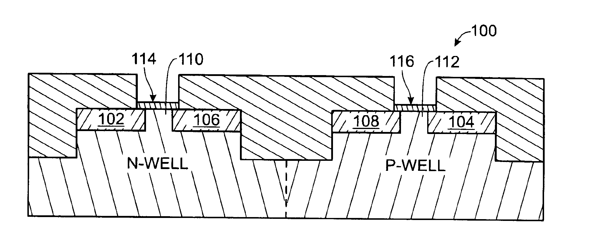
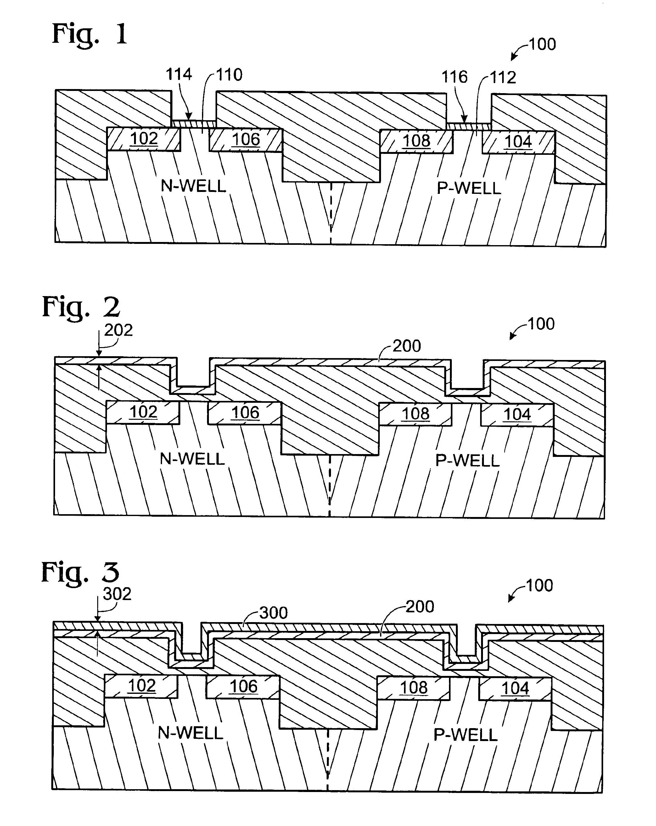
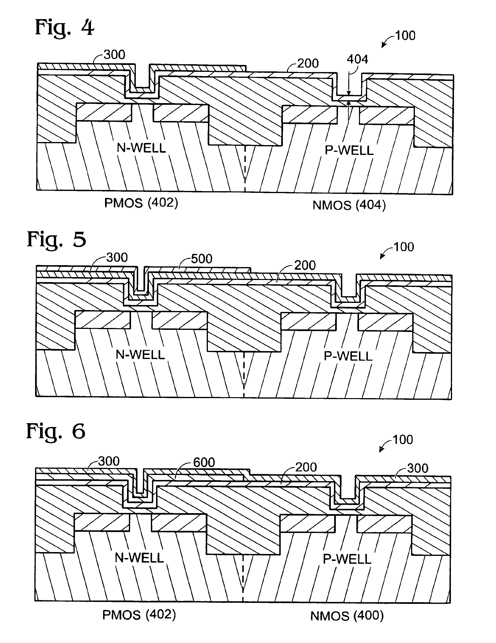
FIGS. 1 through 8 are partial cross-sectional views of steps in the completion of the present invention dual-gate MOSFET with metal gate stack. FIG. 1 depicts the dual-gate MOSFET 100 prior to the deposition of the gate metal layers. The underlying sources 102 and 104, drains 106 and 108, channels 110 and 112, and gate dielectric layers 114 and 116 may be formed by any conventional process.

FIG. 2 depicts the dual-gate MOSFET 100 of FIG. 1 after the deposition of a first metal layer 200. The first metal layer 200 can be deposited to a desired first thickness 202, typically less than 200 Å, using any conventional process. Depending on the desired gate work functions, the composition of the first thin film 200 can be an elemental metal such as W, Ti, or Ta, binary materials such as Ta—N or Ti—N, or compounds consisting of more than two elements.

FIG. 3 depicts the dual-gate MOSFET 100 of FIG. 2 following the deposition of a second metal layer 300. The second metal layer is deposited to ...


PUM

PropertyMeasurementUnit
threshold voltageaaaaaaaaaa
thicknessaaaaaaaaaa
thicknessesaaaaaaaaaa

Abstract

A dual-gate MOSFET with metal gates and a method for setting threshold voltage in such a MOSFET is provided. The method comprises: forming a gate oxide layer overlying first and second channel regions; forming a first metal layer having a first thickness overlying the gate oxide layer; forming a second metal layer having a second thickness overlying the first metal layer first thickness; selectively removing the second metal layer overlying the first channel region; forming a third metal layer; establishing a first MOSFET with a gate work function responsive to the thicknesses of the first and third metal layer overlying the first channel region; and, establishing a second MOSFET, complementary to the first MOSFET, with a gate work function responsive to the combination of the thicknesses of the first, second, and third metal layers overlying the second channel region.

Description

BACKGROUND OF THE INVENTION1. Field of the InventionThis invention generally relates to integrated circuit (IC) fabrication and, more particularly, to a system and method for setting threshold voltages using stacked metal gate structures.2. Description of the Related ArtThe threshold voltages (Vth) of the NMOS and PMOS components in a complementary metal oxide semiconductor (CMOS) circuit largely dictate the speed, standby current, and operating current performance characteristics. The Vth must be set to maximize the “on” current, while minimizing the “off” current. Usually this is a trade off that is determined by the circuit design and application. Typically, the Vth is adjusted through the fine-tuning of the doping level in the channel region of the transistors with a Vth adjust implant. As the feature size of transistors continues to scale down, the struggle to minimize short channel effects, and reduce punchthrough and drain-induced barrier lowering with implantations and annea...

Claims


Application Information

Patent Timeline
Patent Type & Authority Patents(United States)
IPC IPC(8): H01L21/70H01L21/02H01L29/66H01L29/78H01L21/336H01L21/8238H01L29/40H01L29/49H01L21/28H01L27/092H01L29/423
CPCH01L21/823842H01L29/495H01L29/4958H01L29/4966H01L29/66583H01L29/78H01L2924/0002H01L2924/00H01L27/092
Inventor GAO, WEICONLEY, JR., JOHN F.ONO, YOSHI
Owner SHARP LAB OF AMERICA INC
Why Eureka
Try Eureka