Nickel silicide with reduced interface roughness

a technology of silicide and nickel, applied in the field of self-aligned silicide (salicide) technology, can solve the problems of inability to accurately form discreet devices on semiconductor substrates exhibiting the requisite reliability, more limiting circuit operating speed, undesired interface roughness, etc., and achieve the effect of reducing roughness and reducing roughness

Inactive Publication Date: 2005-03-29
ADVANCED MICRO DEVICES INC
View PDF12 Cites 11 Cited by
  • Summary
  • Abstract
  • Description
  • Claims
  • Application Information

AI Technical Summary

Benefits of technology

An advantage of the present invention is a semiconductor device comprising nickel silicide layers and reduced roughness at the interface between the nickel silicide layer and underlying silicon.
Another advantage of the present invention is a method of manufacturing a semiconductor device having reduced roughness at the interface between nickel silicide layers and underlying silicon.
A further advantage of the present invention is a method of manufacturing a semiconductor device having nickel silicide contacts on a gate electrode and associated source/drain regions without bridging therebetween along insulative sidewall spacers, notably silicon nitride sidewall spacers.
An add

Problems solved by technology

As integrated circuit geometries continue to plunge into the deep sub-micron regime, it becomes increasingly more difficult to accurately form discreet devices on a semiconductor substrate exhibiting the requisite reliability.
The higher the value of the RxC product, the more limiting the circuit operating speed.
Upon conducting experimentation and investigation to implement nickel silicide formation, it was discovered that the high resistance nickel disilicide phase (NiSi2) is formed on doped silicon and generates an undesirably rough interface therebetween.
Such interface roughness adversely impacts resistivity and capacitance, and can lead to spiking into the source/drain region or through the gate dielectric layer.
This problem can become particularly acute in silicon-on-insulator (SOI) structures wherein such spiking c

Method used


Image

  • Nickel silicide with reduced interface roughness
  • Nickel silicide with reduced interface roughness
  • Nickel silicide with reduced interface roughness

Examples


Embodiment Construction

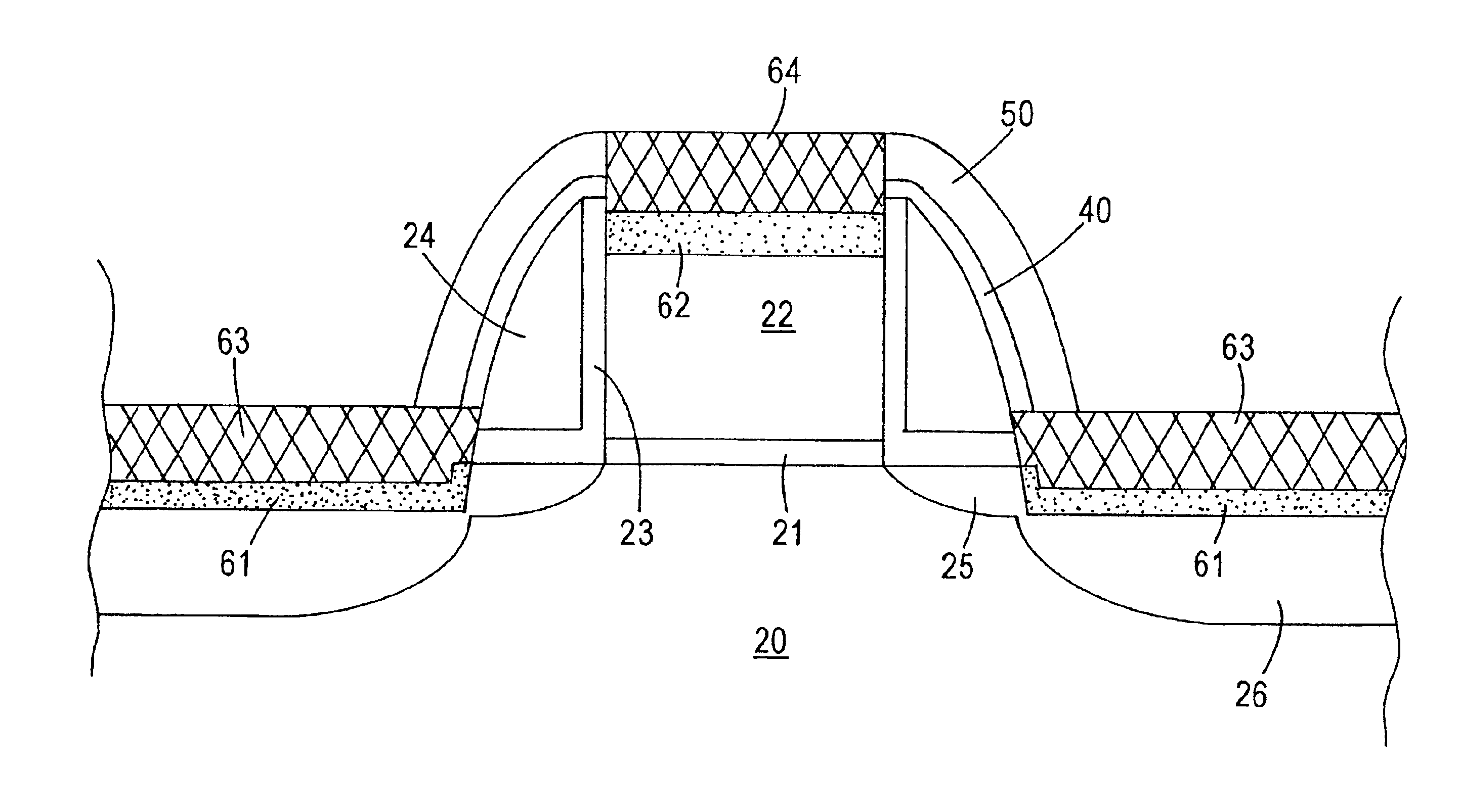
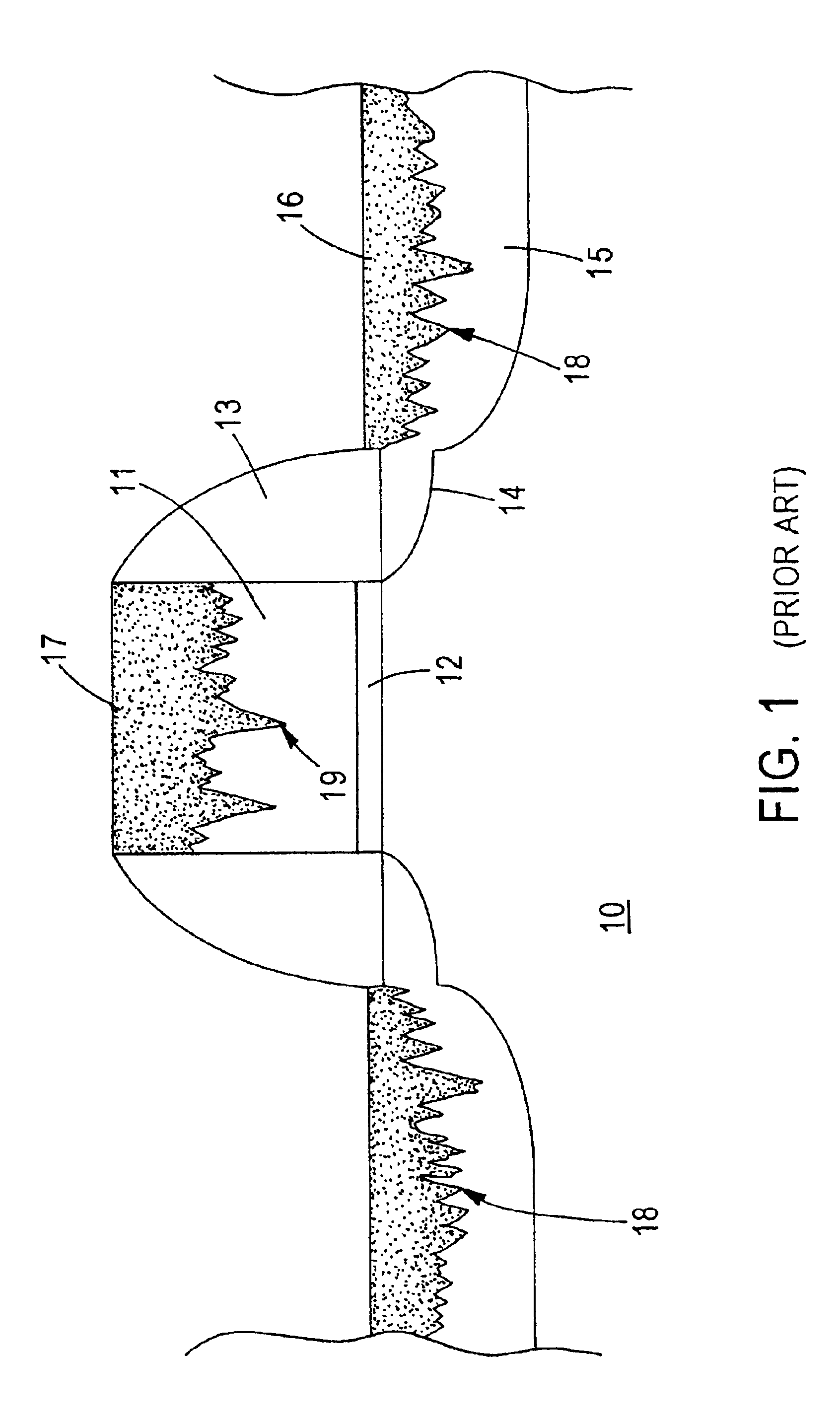
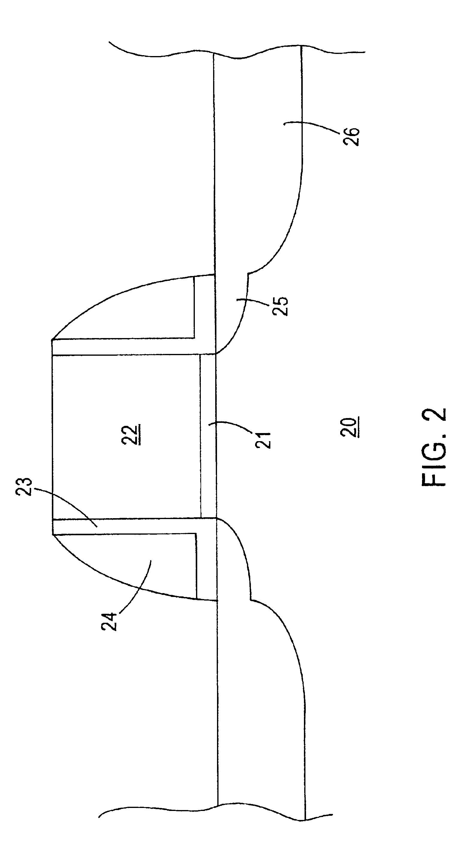
The present invention addresses and solves problems attendant upon implementing conventional salicide technology employing nickel as the metal for silicidation. Such problems include the formation of an extremely rough interface between nickel silicide layers and underlying silicon, which roughness can lead to spiking and penetration into the source / drain regions, as well as spiking through a gate dielectric layer. Further problems include rapid consumption of silicon in the gate electrode which would destroy the known work function of polycrystalline silicon and highly reliable polycrystalline silicon / silicon oxide interface. Additional problems include nickel silicide bridging along the surface of silicon nitride sidewall spacers between the nickel silicide layer on the gate electrode and nickel silicide layers on associated source / drain regions. It is believed that nickel silicide bridging stems from the reaction nickel with dangling silicon bonds in the silicon nitride sidewall ...


PUM


Abstract

Nickel silicide formation with significantly reduced interface roughness is achieved by forming a diffusion modulating layer between the underlying silicon and nickel silicide layers. Embodiments include ion implanting nitrogen into the substrate and gate electrode, depositing a thin layer of titanium or tantalum, depositing a layer of nickel, and then heating to form a diffusion modulating layer containing nitrogen at the interface between the underlying silicon and nickel silicide layers.

Description

TECHNICAL FIELDThe present invention relates to the fabrication of semiconductor devices, particularly to self-aligned silicide (salicide) technology, and the resulting semiconductor devices. The present invention is particularly applicable to ultra large scale integrated circuit (ULSI) systems having features in the deep sub-micron regime.BACKGROUND ARTAs integrated circuit geometries continue to plunge into the deep sub-micron regime, it becomes increasingly more difficult to accurately form discreet devices on a semiconductor substrate exhibiting the requisite reliability. High performance microprocessor applications require rapid speed of semiconductor circuitry. The speed of semiconductor circuitry varies inversely with the resistance (R) and capacitance (C) of the interconnection system. The higher the value of the RxC product, the more limiting the circuit operating speed. Miniaturization requires long interconnects having small contacts and small cross-sections. Accordingly,...

Claims


Application Information

Patent Timeline
IPC IPC(8): H01L21/285H01L23/52H01L21/00H01L21/44H01L21/28H01L21/02H01L23/48H01L21/336H01L29/40H01L21/265H01L29/78H01L29/786
CPCH01L21/28052H01L21/28518H01L21/26506H01L29/6659H01L29/665H01L21/24
Inventor PATON, ERICBESSER, PAUL RAYMONDCHAN, SIMON S.HAUSE, FRED
Owner ADVANCED MICRO DEVICES INC
Why Eureka
Try Eureka