Semiconductor device having an insulation film with reduced water content

a technology of semiconductor devices and insulation films, applied in the direction of semiconductor devices, electrical devices, transistors, etc., can solve the problems of deviation of threshold voltage, drain current becomes no longer controllable by gate voltage, and extreme miniaturized semiconductor devices tend to suffer from so-called short-channel effect, etc., to reduce the resistance of very shallow diffusion regions and the effect of h2o

Inactive Publication Date: 2005-04-12
FUJITSU SEMICON LTD
View PDF27 Cites 6 Cited by
  • Summary
  • Abstract
  • Description
  • Claims
  • Application Information

AI Technical Summary

Benefits of technology

According to the present invention, the amount of H2O in the first insulation film is successfully reduced by the gettering action of P or B that is contained in the PSG or BPSG forming the first insulation film. Even when a high-temperature CVD process is used for forming the first

Problems solved by technology

On the other hand, such an extremely miniaturized semiconductor device tends to suffer from the problem of so-called short-channel effect, which appears conspicuously in such a miniaturized device having a short gate length, due to the deviation from the classical gradual channel approximation model.
When a short-channel effect appears, there arise problems such as deviation of threshold voltage.
In the worst case, the drain current becomes no longer controllable by the gate voltage.
In such a conventional process of forming a silicide layer, however, there is a substantial risk that the etching process, used in the step of FIG. 1G for removing the SiN film 4 from the bottom of the contact holes 5A and 5B, may proceed further to the diffusion region 1C or 1D and cause

Method used


Image

  • Semiconductor device having an insulation film with reduced water content
  • Semiconductor device having an insulation film with reduced water content
  • Semiconductor device having an insulation film with reduced water content

Examples


first embodiment

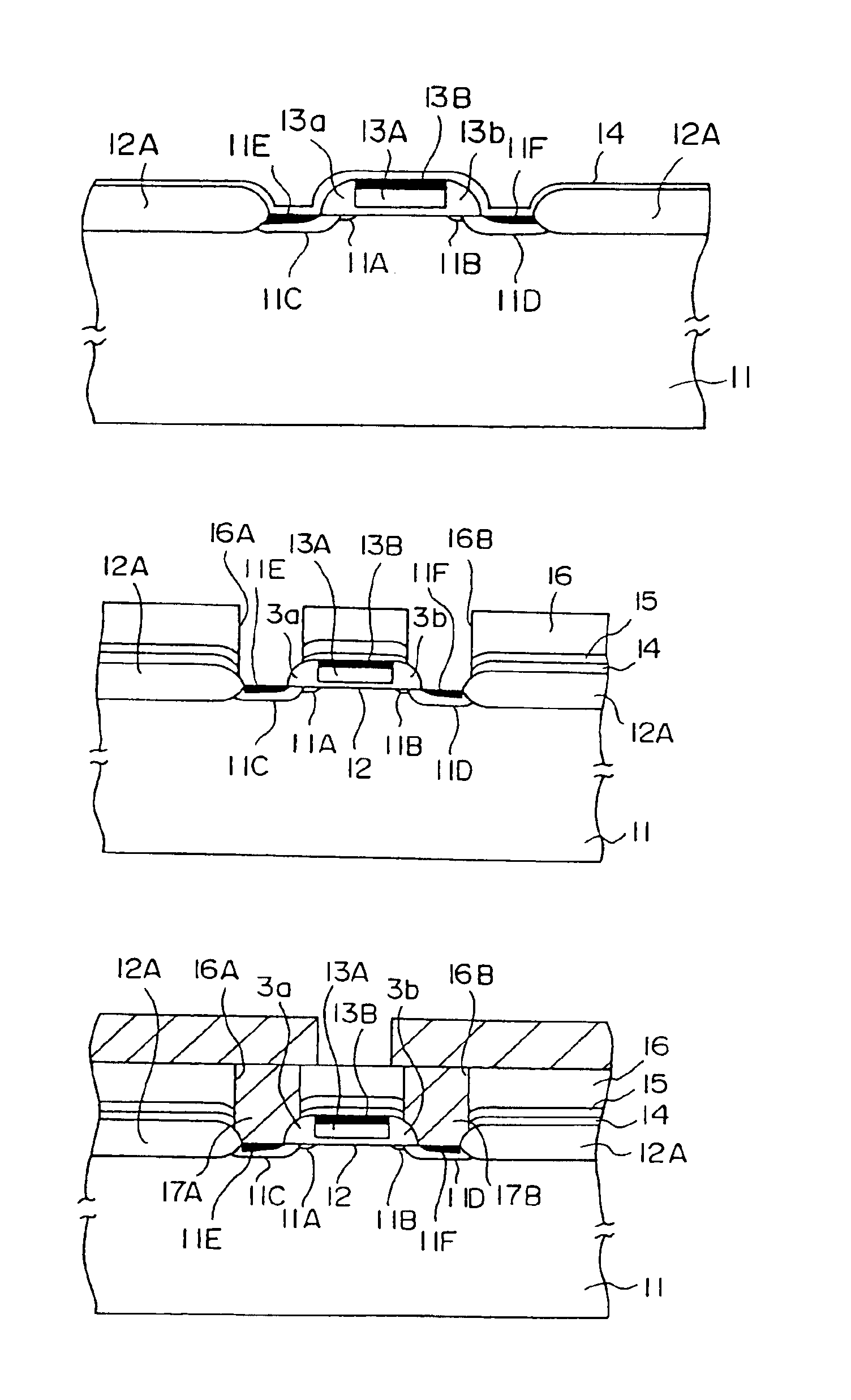
FIGS. 15A-15I show a fabrication process of a MOS transistor according to a first embodiment of the present invention.

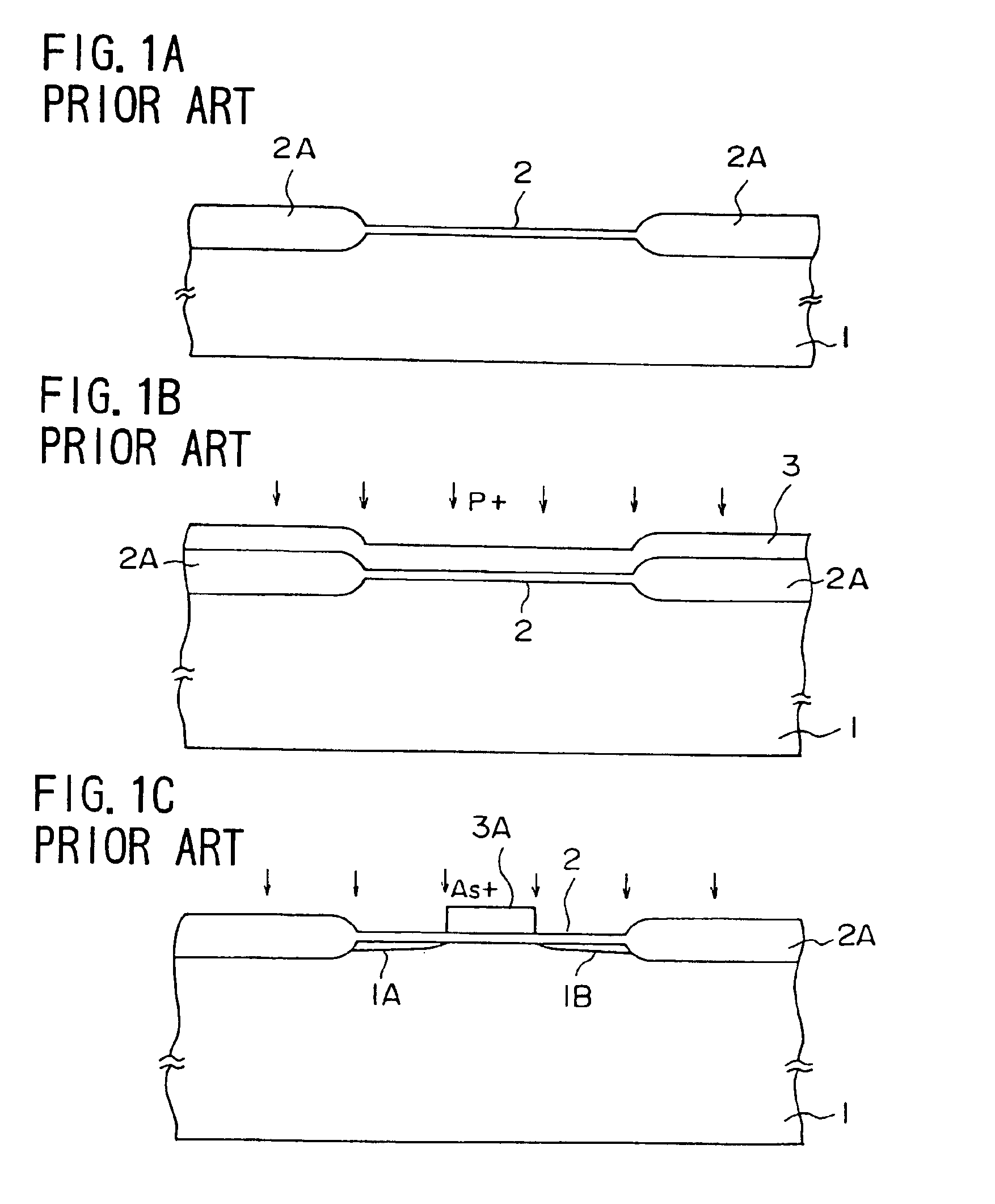
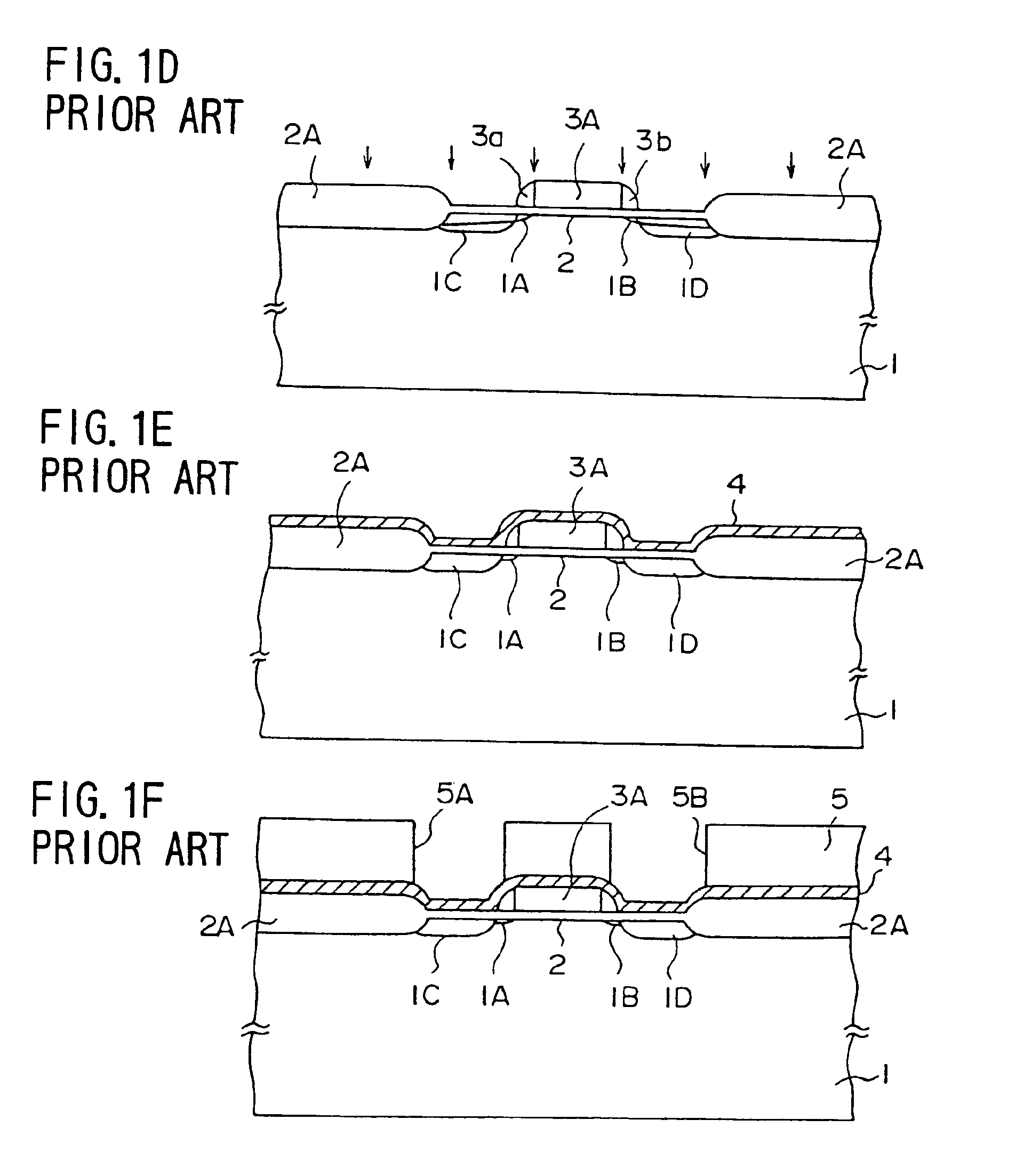
Referring to FIG. 15A, a gate oxide film 12 and a field oxide film 12A are formed on a p-type Si substrate 11 corresponding to the Si substrate 1 of FIG. 1A, and a polysilicon layer 13 is deposited on the structure of FIG. 15A in the step of FIG. 15B. The polysilicon layer 13 thus deposited is then doped to the n+-type by an ion-implantation of P+ ions and patterned in the step of FIG. 15C to form a gate electrode 13A. The ion implantation process of FIG. 15B may be conducted under an acceleration voltage of 20 keV with a dose of 4×1015 cm−2. In the step of FIG. 15C, an ion implantation process of As+ is further conducted while using the gate electrode 13A as a mask, to form shallow diffusion regions 11A and 11B of the n+-type at both lateral sides of the gate electrode 13A by a self-alignment process. The ion implantation process of FIG. 15C may be conducted under a...

second embodiment

FIGS. 16A-16O show a fabrication process of a semiconductor device according to a second embodiment of the present invention.

Referring to FIG. 16A, a Si substrate 21 of the p-type or n-type is covered by a native oxide film 22N, and an SiN mask 23A as well a an SiN mask 23B are provided on the substrate 21 such that the SiN mask 23A protects an NMOS region on which an NMOS transistor is to be formed. Similarly, the SiN mask 23B protects a PMOS region on which a PMOS transistor is to be formed. The mask 23A and 23B are separated and there is formed a gap between the region for the NMOS transistor and the region for the PMOS transistor. The gap exposes the native oxide film 22N formed on the substrate 21.

Next, in the step of FIG. 16B, the structure of FIG. 16A is subjected to a wet oxidation process to form a field oxide film 23 in correspondence to the foregoing gap typically with a thickness of about 250 nm. Further, a mask M1 is provided in the step of FIG. 16B so as to cover the P...


PUM


Abstract

A semiconductor device having a self-aligned contact hole is formed by providing a side wall oxide film on a gate electrode, covering the gate electrode and the side wall oxide film by an oxide film and further covering the oxide film by a nitride film, wherein the oxide film is formed by a plasma CVD process with a reduced plasma power such that the H2O content in the oxide film is less than about 2.4 wt %.

Description

BACKGROUND OF THE INVENTIONThe present generally relates to semiconductor devices and more particularly to a miniaturized high-speed semiconductor device and a fabrication process thereof.With the development in the art of device miniaturization, the operational speed of field-effect semiconductor devices such as a MOS transistor is increasing every year. On the other hand, such an extremely miniaturized semiconductor device tends to suffer from the problem of so-called short-channel effect, which appears conspicuously in such a miniaturized device having a short gate length, due to the deviation from the classical gradual channel approximation model. When a short-channel effect appears, there arise problems such as deviation of threshold voltage. In the worst case, the drain current becomes no longer controllable by the gate voltage.Thus, it has been practiced in conventional miniaturized field effect semiconductor devices to reduce the thickness of diffusion regions as small as po...

Claims


Application Information

Patent Timeline
IPC IPC(8): H01L21/70H01L21/60H01L21/02H01L21/768H01L21/316H01L21/318H01L21/336H01L21/28H01L29/78
CPCH01L21/02129H01L21/02211H01L21/02271H01L21/02274H01L21/31612H01L21/31625H01L21/76832H01L21/76834H01L21/76895H01L21/76897H01L29/6656H01L21/02164H01L29/7833H01L29/665H01L29/6659
Inventor SUZUKI, KOUSUKEKARAKAWA, KATSUYUKI
Owner FUJITSU SEMICON LTD
Why Eureka
Try Eureka