Semitransparent optical detector including a polycrystalline layer and method of making

a polycrystalline layer and detector technology, applied in the direction of sustainable manufacturing/processing, instruments, final product manufacturing, etc., can solve the problems of increasing cost, increasing the difficulty of linear arrays of lasers to produce in high densities, and increasing the cost of laser testing. achieve the effect of high intensity hea

Inactive Publication Date: 2005-04-12
II VI DELAWARE INC +1
View PDF27 Cites 113 Cited by
  • Summary
  • Abstract
  • Description
  • Claims
  • Application Information

AI Technical Summary

Problems solved by technology

Edge emitting devices have a number of drawbacks: first, each laser takes a relatively large area on the semiconductor wafer, increasing cost; second, lasers cannot be tested until after they have been diced into individual units; third, linear arrays of lasers are more difficult to produce in high densities and two-dimensional arrays are altogether impossible to fabricate.
Semiconductor light sources in general suffer from a number of problems associated with optical power control.
Semiconductor lasers suffer from the fact that their threshold currents—and sometimes their slope efficiencies—can change significantly over operating temperature ranges and with laser age.
This is a problem for a number of reasons.
First, a single operating current cannot be set for the lifetime of the laser, unless it is set sufficiently high that output power will always exceed a desired minimum.
This strategy has drawbacks: first, there may be eye safety issues when a laser is operated at greater than a certain power; second, operating the laser continuously at high power significantly reduces lifetime and further raises temperature, and as a result, threshold current; and finally, at high powers, high and low light output levels may be difficult to distinguish.
Thus a drift in the threshold current during operation can have highly detrimental results for users who wish to attain maximum bandwidth from such lasers while meeting eye safety and power consumption specifications.
These optical power fluctuations are a problem not only for laser diodes or VCSELS; they affect other SLEDs as well, necessitating power control or monitoring for level-sensitive applications.
Thermal control solutions require significant space and power, and although they may be suitable for long-haul communications applications, such solutions are generally unacceptable in local-area or interconnect components where space is at an extreme premium.
Thermally-based solutions do not by themselves solve the problem of laser performance degradation over its operating lifetime.
They can only compensate for changes in the ambient temperature, which, although important, are far from the only factor affecting laser optical output for a given current.
For VCSELs, power monitoring is more complex, because the device does not generally emit light in the rear direction, i.e., through the substrate wafer.
Both of these potential structures have not been used in production devices as a result of the significantly higher manufacturing complexities involved, and because of the fact that they do not directly monitor the same emission modes propagated by the surface-emitting device through its aperture, for example into a communication medium.
Such an array would have even greater power control issues than a single-wavelength array, because processing is slightly different for each laser.
However, this technique has severe drawbacks.
Not only will it result in different average power levels coming from the lasers and, indeed, a higher required overall bias current than necessary in order to insure reliable function over lifetime, but may result in such disparities in power that an eye safety hazard results.
Another major drawback of current backreflection power monitors is the fact that light emanating from the VCSEL is not uniformly measured by the detector.
This poses a problem for an optical monitor that reflects part of the emitted light into a photodiode.
The impractical result is that each VCSEL / monitor unit must be individually calibrated after assembly in order to know the relation between photodiode current and actual optical power produced by the VCSEL.
Moreover, the relative intensities of the modes emitted by a VCSEL will change over temperature and age which means that the conditions observed during calibration may not exist over the entire operating lifetime of the VCSEL, and significant distortions of the power feedback signal may result over time.
Other issues such as the mechanical and optical stability of the semireflective window used to direct light back to the photodetector will affect measurement as well.
For example, dust on the outside of the window may cause significantly higher backreflection, leading to an overestimate of delivered laser power.
However, even with this partial solution, direct integration of the VCSEL with waveguides—or, for that matter, incorporation into any other package that does not easily incorporate a window—is still impossible (assuming a power monitor is required).
One of the VCSEL's potential strengths is that it could be directly coupled to waveguides and fibers, and bonded to a variety of surfaces; this strength of the VCSEL cannot be exploited using conventional technologies.
However, no such device has yet appeared because of numerous problems heretofore thought insurmountable.
Even to experts in the field, the fabrication of devices meeting all these parameters has proven impossible.
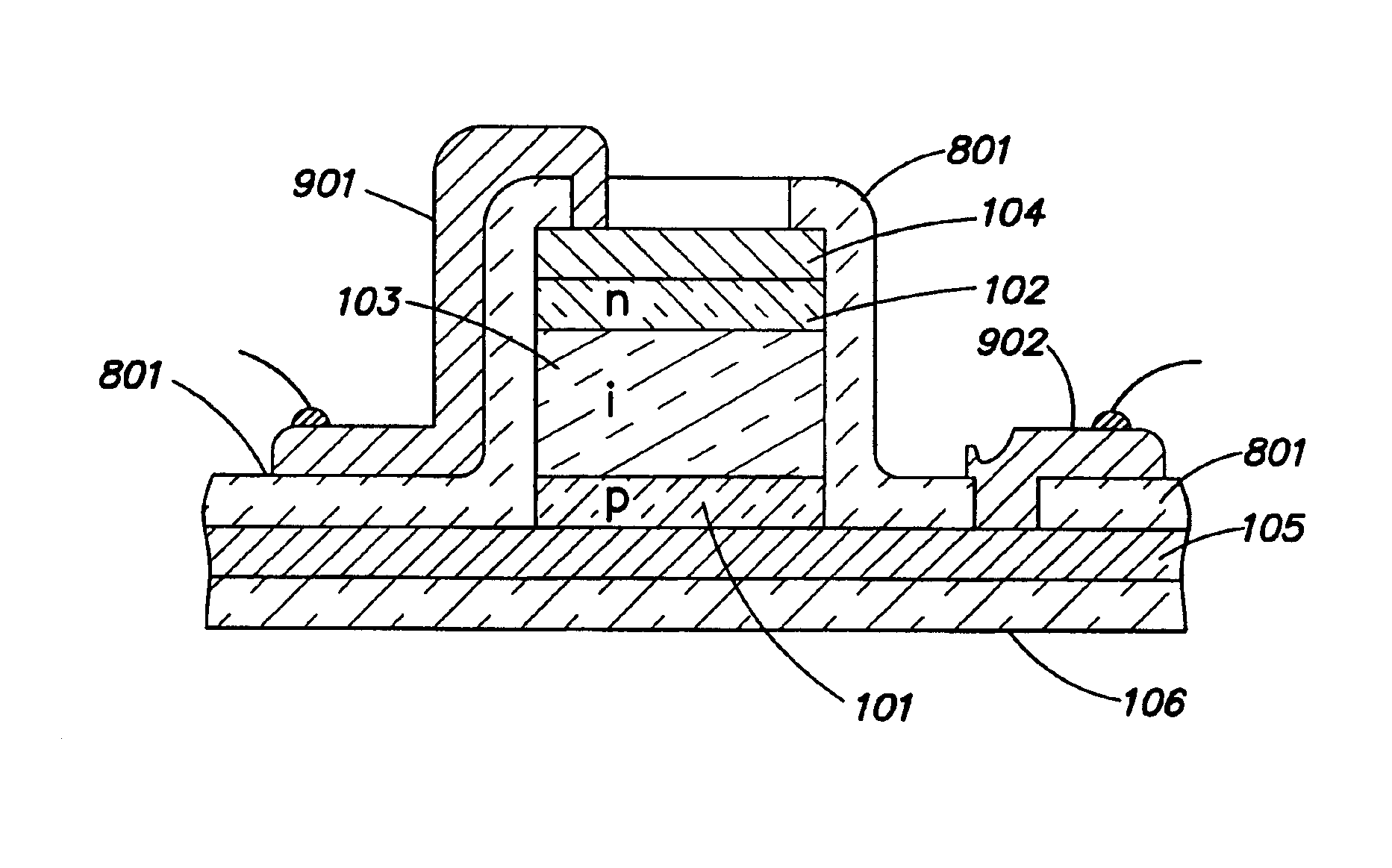
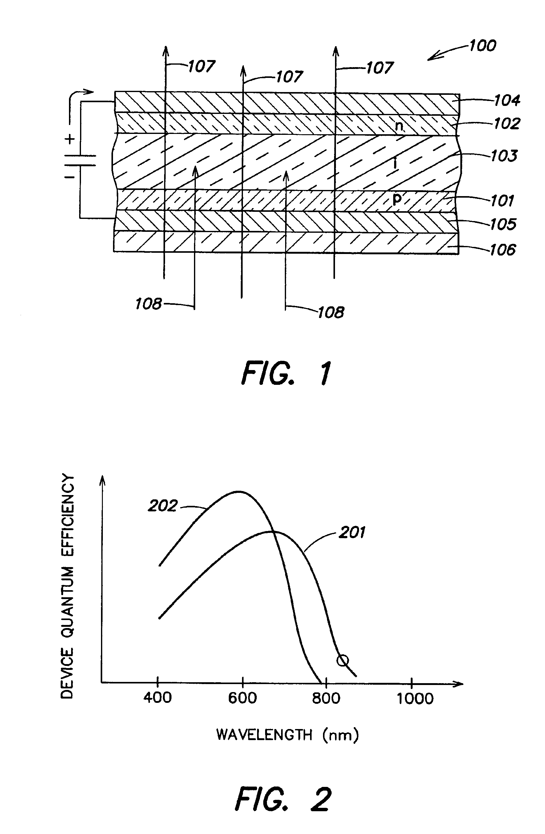
Dark current in photodetectors is a perennial issue, particularly when the photodetector is stretched to meet other specifications such as responsivity at a particular wavelength and partial transparency.
A particular problem is the leakage on the edges of the device.
When the conductor used for this connection is relatively thin when compared to the structure's height and is deposited by a directional method that preferentially deposits on surfaces parallel to the substrate broken connections often result.
An immediate potential solution was to use very thick layers of metal to form the contact once the layer is thick enough it will reach over the edge of the PIN stack; this fix, however, brings with it other problems when working with thin films.
In particular, the film stress induced by such a thick layer will tend to peel off the entire photodetector structure.
When the conductor used for this connection is relatively thin when compared to the structure's height, and is deposited by a directional method that preferentially deposits on surfaces parallel to the substrate, broken connections often result.
Another problem is because the entire PIN structure was extended for large areas under the insulating layer and contacts i.e., areas that do not contribute to the intended photoresponse of the device, the dark current exhibited by the devices rose significantly for two reasons: (1) there is a much larger bulk of PIN stack that will produce purely thermal currents, particularly at higher temperatures and (2) the leakage currents produced along the extended edges of the structure rise.

Method used


Image

  • Semitransparent optical detector including a polycrystalline layer and method of making
  • Semitransparent optical detector including a polycrystalline layer and method of making
  • Semitransparent optical detector including a polycrystalline layer and method of making

Examples


Embodiment Construction

The present invention is now illustrated by the following detailed description of a number of embodiments and aspects thereof.

In illustrating the present invention, some basic materials, basic structures, advanced material, advanced structures and complete devices are now described. The various materials and structures are described in relation to a number of preferred combinations. However, it will then be apparent that other combinations of the same materials and structures are suggested by the described combinations. All such combinations are contemplated as within the scope of this disclosure.

Basic Materials

In order to build semitransparent optical detectors, semitransparent materials are required. In order to use conventional crystalline silicon semiconductors one would need to cut a single-crystal wafer so thin that most of the monitored beam could pass through the wafer and a detector patterned on it using conventional integrated-circuit processes. The advantage of this metho...


PUM

PropertyMeasurementUnit
temperatureaaaaaaaaaa
temperaturesaaaaaaaaaa
reverse bias voltagesaaaaaaaaaa

Abstract

Materials suitable for fabricating optical monitors include amorphous, polycrystalline and microcrystalline materials. Semitransparent photodetector materials may be based on silicon or silicon and germanium alloys. Conductors for connecting to and contacting the photodetector may be made from various transparent oxides, including zinc oxide, tin oxide and indium tin oxide. Optical monitor structures based on PIN diodes take advantage of the materials disclosed. Various contact, lineout, substrate and interconnect structures optimize the monitors for integration with various light sources, including vertical cavity surface emitting laser (VCSEL) arrays. Complete integrated structures include a light source, optical monitor and either a package or waveguide into which light is directed.

Description

BACKGROUND1. Field of the InventionThe present invention relates generally to devices for monitoring the performance of optical systems. The present invention relates more particularly to devices for monitoring the performance of laser light sources used in communications and computation systems.2. Related ArtThe vertical cavity surface-emitting laser (VCSEL) is a relatively recent innovation in laser technology. It is part of a general class of devices called “surface emitting light emitting devices” (SLEDs) that have significant manufacturing and packaging advantages over conventional edge-emitting devices.Semiconductor diode lasers have been produced for over a decade and are used extensively in both communications and in optical storage devices such as compact disks (CDs) and digital versatile disks (DVDs). The vast majority of these devices, however, rely on edge-emitting, e.g., Fabry-Perot or distributed feedback (DFB), lasers. These lasers are constructed on semiconductor waf...

Claims


Application Information

Patent Timeline
Patent Type & Authority Patents(United States)
IPC IPC(8): H01L29/04H01L29/02H01L31/036H01L31/06H01L31/075H01L31/0368H01L31/18
CPCH01L31/03682H01L31/1016H01L31/1872Y02E10/546H01L2224/48091H01L2224/48465H01S5/0683H01S5/423H01S5/02325Y02E10/548Y02P70/50H01L2924/00014
Inventor WAGNER, SIGURDWAGNER, MATTHIASMA, EUGENE Y.PAYNE, ADAM M.
Owner II VI DELAWARE INC
Why Eureka
Try Eureka