Photoelectrochemical undercut etching of semiconductor material

a technology of photoelectrochemical and semiconductor materials, applied in the direction of semiconductor devices, electrical equipment, decorative arts, etc., can solve the difficulty of identifying reliable and controllable wet etchants, and the anisotropy of pec etching, etc., to achieve small energy shift and strong undercut

Inactive Publication Date: 2005-04-26
RGT UNIV OF CALIFORNIA
View PDF7 Cites 27 Cited by
  • Summary
  • Abstract
  • Description
  • Claims
  • Application Information

AI Technical Summary

Benefits of technology

[0019]The present invention enables the ready lift-off of semiconductor devices, which is particularly useful when the substrate is sapphire or other inert material. Significantly the present invention provides a geometry that can produce strong undercuts and new morphologies, enabling the fabrication of a variety of MOEMS and MEMS not heretofore practical with group III nitrides. Lateral and undercutting etching of the PEC method of the present invention has resulted in the fabrication of group III nitride cantilever and membrane structures not heretofore available. The present invention can enable the construction of dynamically tunable transitions on a device scale and can be applied in a variety of devices, including transistors (e.g., HEMTs), light emitters (e.g., LEDs, lasers), and detectors. Strains on the order of 10−4 produce a very small energy shift, on the order of a few meV. The inventors are aware of no other examples of strain-tuned device structures, in any material system.

Problems solved by technology

However, the group III nitrides are distinguished by their unusual chemical stability, making it difficult to identify reliable and controllable wet etchants.
Clearly either case has aspects which may not be favorable for the fabrication of an arbitrary device.
PEC etching's anisotropy, however, derives from the control of the requisite above-bandgap illumination.
However, while such a strong and rapid anisotropy may be useful for mesa- or via-etching, it does not provide undercut etching.
However these substrates create or worsen many problems in the final device.
One such problem that is made worse is thermal resistance.
Because these substrates are very hard and quite chemically inert, it is difficult to lift off the GaN device or remove it through decomposition of the substrate in a conventional etching processes.

Method used


Image

  • Photoelectrochemical undercut etching of semiconductor material
  • Photoelectrochemical undercut etching of semiconductor material
  • Photoelectrochemical undercut etching of semiconductor material

Examples


example 1

[0066]A Current Apertured Vertical Electron Transistor (CAVET) 64 is fabricated by the application of this invention to a target layer located just below the gate of a vertical transistor structure, as shown in FIG. 6. The structure is grown to include a target layer 66 of indium gallium nitride between the source 68 and the drain 70. This is then laterally etched using the techniques of this invention to produce the undercut structure shown in FIG. 6 The resulting aperture between the source 68 and the drain 70 enhances the pinch-off of the gate 72 by providing a highly insulating air-gap 74 which confines the current to the area below the gate 72, while retaining a larger area for use as source and drain contacts to either side of the aperture.

example 2

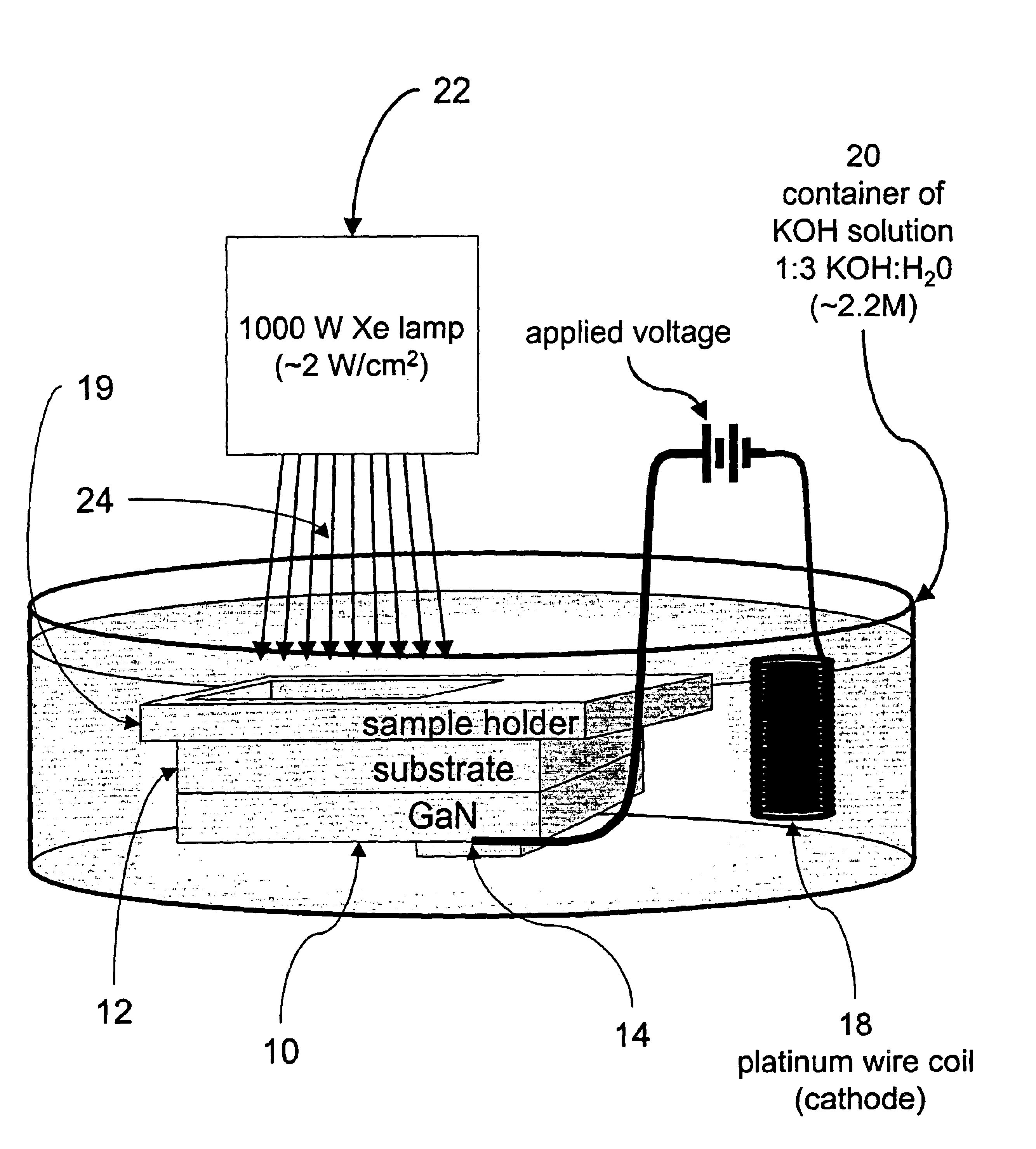
[0067]Cantilevers formed of gallium nitride are fabricated by including a target layer of indium gallium nitride in the growth of a thicker layer of gallium nitride. This is then patterned and etched by a vertical etch of prior art to define the area of the cantilever, and its supporting base. The indium gallium nitride layer is then partially etched by the technique shown in FIG. 5, using the mask 62 shown to define which areas are separated from the lower layer of gallium nitride. A broad range of conditions have been shown to be suitable for such an etch. In the case shown a KOH concentration of 2.2 molar was employed, as was a simple platinum-wire cathode, and a relevant illumination intensity of 2 watts per square centimeter.

[0068]The resulting cantilevers are shown in a scanning electron micrograph in FIG. 7A, and schematically before and after lateral etching in FIGS. 7B and C respectively. The strain state in the as grown material is shown in 7B, It is the relaxation of this...

example 3

[0070]The procedure of Example 2 was followed but a thin layer of indium gallium nitride (a quantum well) was included near the top of the cantilever. Plots showing resonant responses of the fabricated GaN and InGaN cantilevers are shown in FIG. 7D, and are labeled InGaN / GaN cantilevers.


PUM

PropertyMeasurementUnit
thicknessaaaaaaaaaa
thicknessaaaaaaaaaa
thicknessaaaaaaaaaa

Abstract

Photoelectrochemical (PEC) etching is restricted to a group III nitride semiconductor-barrier interface to laterally etch or undercut the target group III nitride. The barrier interface is provided by the transparent sapphire substrate on which the target group III nitride is epitaxially grown or by a layer of material in intimate contact with the target group III nitride material and having a bandgap sufficiently high to make it resistant to PEC etching. Due to the first orientation in which this effect was first observed, it has been named backside-Illuminated photoelectrochemical (BIPEC) etching. It refers to a preferential etching at the semiconductor-barrier layer interface. The assembly can be exposed to light from any direction to effectuate bandgap-selective PEC etching. An opaque mask can be applied to limit the lateral extent of the photoelectrochemical etching.

Description

CROSS REFERENCE TO RELATED APPLICATIONS[0001]This application claims the benefit of U.S. Provisional Application No. 60 / 317,419, filed Sep. 4, 2001, and which is incorporated herein by reference.STATEMENT REGARDING FEDERALLY SPONSORED RESEARCH OR DEVELOPMENT[0002]This invention was made with Government Support under Contract No. 14-96-1-1215, awarded by the Office of Naval Research. The Government has certain rights in this invention.BACKGROUND OF THE INVENTION[0003]1. Field of the Invention[0004]This invention relates in general to a method of processing a semiconductor wafer, and more particularly, to a photoelectrochemical etching process.[0005]2. Description of Related Art[0006]There has been impressive progress in the growth of high quality GaN epitaxial layers and in their utilization for high performance optical devices. The group III nitrides hold great promise as the basis for a variety of high performance optoelectronic and electronic devices. GaN-based materials are well ...

Claims


Application Information

Patent Timeline
Patent Type & Authority Patents(United States)
IPC IPC(8): H01L21/02H01L21/00H01L21/302H01L21/461H01L21/3063
CPCH01L21/30635Y10S438/962
Inventor HU, EVELYN L.STONAS, ANDREAS R.
Owner RGT UNIV OF CALIFORNIA
Why Eureka
Try Eureka