Laser annealing apparatus and annealing method of semiconductor thin film

a technology of semiconductor thin film and laser annealing apparatus, which is applied in the direction of manufacturing tools, crystal growth process, polycrystalline material growth, etc., can solve the problems of large energy loss, reduced short wavelength of laser beam to about 20 microns, and prone to energy change damage to silicon film, etc., to achieve good annealing, small energy loss, and high mobility

Inactive Publication Date: 2005-08-04
HITACHI DISPLAYS
View PDF8 Cites 50 Cited by
  • Summary
  • Abstract
  • Description
  • Claims
  • Application Information

AI Technical Summary

Benefits of technology

[0009] To solve the problems in the background art, an object of the invention is to provide a laser annealing method and a laser annealing apparatus in which a laser beam is shaped into a long and narrow beam efficiently without energy loss so that a silicon film exhibiting high mobility in a wide energy condition range can be formed.
[0011] In the laser annealing method and laser annealing apparatus according to the invention, a laser beam can be shaped into a long and narrow beam with a small energy loss when a diffractive optical element simple in structure or a combination of a Powell's lens and a cylindrical lens is used as a homogenizer (beam shaper).
[0012] In addition, when the shaped beam is reductively projected by an imaging lens, a long and narrow beam having a required short dimension (or scanning-direction dimension) can be obtained. A value of from 2 to 10 microns or preferably a value of from 2 to 4 microns can be achieved as the short dimension of the beam obtained on this occasion. When the scanning speed is selected to be preferably in a range of from 300 to 1000 mm / s, further preferably in a range of from 500 to 1000 mm / s, good annealing can be performed so that belt-like crystals can be formed in the laser-irradiated region.
[0013] According to the invention, a silicon film of high mobility can be obtained stably, so that a thin film semiconductor device substrate of good performance can be obtained. When the invention is applied to production of a display device represented by a liquid crystal display device or an organic EL display device, so-called “system-in” can be achieved.

Problems solved by technology

That is, in the conventional technique, there is a problem that the energy loss is large because a multi-lens array or kaleidoscope complex in structure is used as a homogenizer (beam shaper) for shaping a solid-state laser beam such as the second harmonic of a CW YAG laser beam used into a long and narrow beam or a rotary diffusing plate is used for reducing coherence.
In addition, there is a problem that the silicon film is apt to be damaged by change in energy because the energy condition range in which good laterally grown crystals can be obtained is narrow though a required region is irradiated with the laser beam at a scanning speed of about 100 mm / s after the laser beam is shaped into a long and narrow beam so that the short dimension of the laser beam is reduced to about 20 microns.

Method used


Image

  • Laser annealing apparatus and annealing method of semiconductor thin film
  • Laser annealing apparatus and annealing method of semiconductor thin film
  • Laser annealing apparatus and annealing method of semiconductor thin film

Examples


Embodiment Construction

[0027] The present invention will be described below in detail with reference to the drawings showing respective embodiments thereof.

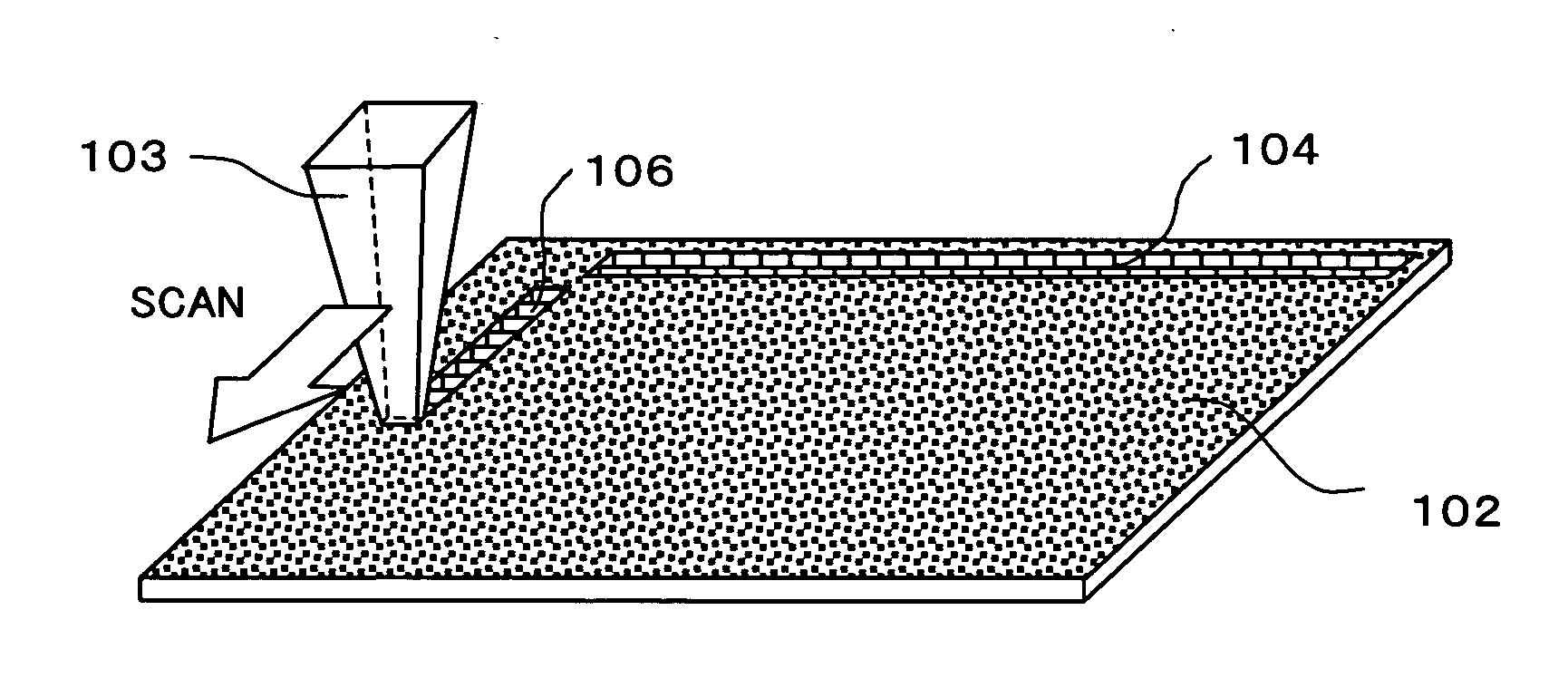
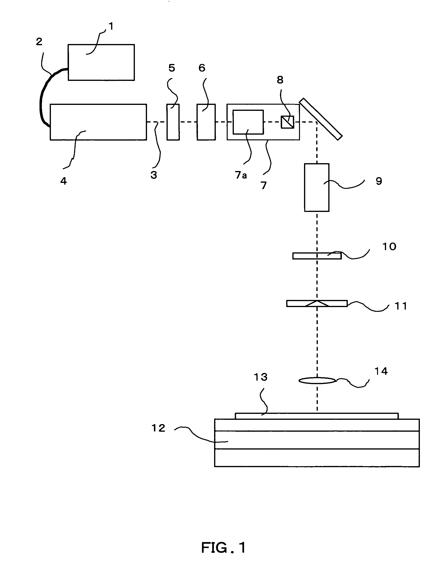
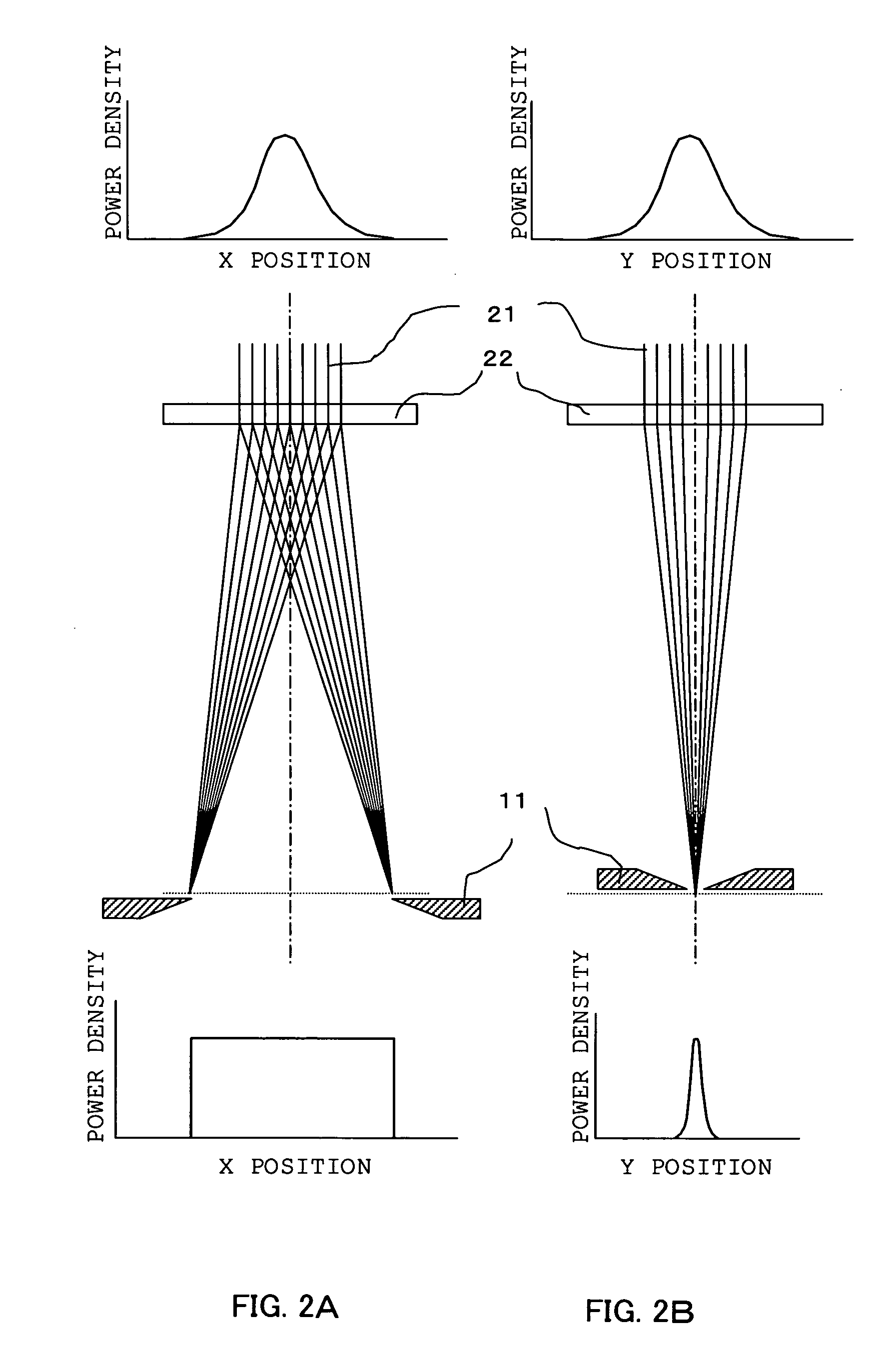
[0028]FIG. 1 is a diagram showing the optical configuration of a laser annealing apparatus according to an embodiment of the invention. The annealing apparatus comprises a laser oscillator 4, a shutter 5, a continuously variable transmittance neutral-density (ND) filter 6, a modulator 7, a beam expander (beam reducer) 9, a beam shaper 10, a rectangular opening slit 11, and an imaging lens 14. The laser oscillator 4 is connected to an excitation laser diode (LD) 1 by a fiber 2 and generates a continuous-wave (CW) laser beam 3. The shutter 5 switches the laser beam 3 on and off. The continuously variable transmittance ND filter 6 controls the energy of the laser beam 3. The modulator 7 temporally modulates in amplitude the laser beam 3 output from the laser oscillator 4 to achieve temporal amplitude modulation of pulsation or energy. The beam expander (...


PUM

PropertyMeasurementUnit
sizeaaaaaaaaaa
sizeaaaaaaaaaa
speedaaaaaaaaaa

Abstract

When a laser bean temporally modulated in amplitude by a modulator is shaped into a long and narrow beam by a beam shaper, the scanning-direction size of the long and narrow beam shaped by the beam shaper is selected to be in a range of from 2 to 10 microns, preferably in a range of from 2 to 4 microns and the scanning speed of the beam is selected to be in a range of from 300 to 1000 mm / s, preferably in a range of from 500 to 1000 m / s. As a result, damage of the silicon thin film can be suppressed while energy utilizing efficiency of the laser beam can be improved. Accordingly, laterally grown crystals (belt-like crystals) improved in throughput can be obtained on a required region of a substrate scanned and irradiated with the laser beam.

Description

BACKGROUND OF THE INVENTION [0001] The present invention relates to a laser annealing method and a laser annealing apparatus adapted for improvement of film quality and magnification or single-crystallization of crystal grains by applying a laser beam on an amorphous or polycrystalline semiconductor film formed on an insulating substrate. [0002] At present, in a display device such as a liquid crystal display device or an organic electroluminescence (EL) display device, an image is formed by switching of pixel transistors (thin-film transistors) each formed from an amorphous or polycrystalline silicon film on a substrate such as a glass substrate or a fused quartz substrate. If a driver circuit for driving each pixel transistor can be formed together with the pixel transistor on the substrate, there is expectation that reduction in production cost and improvement in reliability will be attained remarkably. When a silicon film serving as an active layer of a transistor (thin film tra...

Claims


Application Information

Patent Timeline
Patent Type & Authority Applications(United States)
IPC IPC(8): H01L21/324B23K26/073C30B13/24C30B29/06H01L21/20H01L21/268H01L29/04H01L29/786
CPCB23K26/0738C30B13/24H01L29/78675H01L21/2026H01L29/04C30B29/06H01L21/02683H01L21/02422H01L21/02678H01L21/02532H01L21/02691H01L21/324H01L21/20
Inventor HONGO, MIKIOYAZAKI, AKIOHATANO, MUTSUKONODA, TAKESHITAKASAKI, YUKIO
Owner HITACHI DISPLAYS
Why Eureka
Try Eureka