Process and apparatus for epitaxially coating a semiconductor wafer and epitaxially coated semiconductor wafer

a technology of epitaxial coating and semiconductor wafer, applied in the direction of coating, crystal growth process, polycrystalline material growth, etc., can solve the problems of increasing metal contamination, unsatisfactory solution of autodoping problem, and inability to escape elements, etc., to avoid autodoping

Inactive Publication Date: 2005-05-03
SILTRONIC AG
View PDF12 Cites 1 Cited by
  • Summary
  • Abstract
  • Description
  • Claims
  • Application Information

AI Technical Summary

Benefits of technology

[0013]Therefore, it is an object of the present invention to provide a process for depositing an epitaxial layer on a semiconductor wafer which makes it possible to substantially avoid autodoping without the wafer back surface previously being provided with a protective layer.
[0014]This object is achieved according to the invention by a process for epitaxially coating the front surface of a semiconductor wafer in a CVD reactor, the front surface of the semiconductor wafer being exposed to a process gas which contains a source gas and a carrier gas, and the back surface of the semiconductor wafer being exposed to a displacement gas, wherein the displacement gas contains no more than 5% by volume of hydrogen, with the result that diffusion of dopants out of the back surface of the semiconductor wafer, which is intensified by hydrogen, is substantially avoided.
[0017]It has been found that hydrogen plays an important role in autodoping. For example, with boron or arsenic it forms complexes which diffuse rapidly into silicon. In addition, at the temperatures which are customary in epitaxy the hydrogen removes silicon, which additionally liberates dopant. When the wafer back surface comes into contact with hydrogen during the epitaxy process, therefore, the dopant may emerge from the wafer back surface to an increased extent. The dopant can then be conveyed over the wafer edge and incorporated radially inhomogenously in the epitaxial layer on the wafer front surface. If contact between the wafer back surface and hydrogen is avoided, as in the process according to the invention, outdiffusion of dopants and therefore autodoping are substantially suppressed.
[0018]By contrast, the processes which are disclosed in WO 01 / 86034 A2 and WO 01 / 86035 A1 continue to allow outdiffusion of the substrate dopant, since hydrogen or hydrogen-containing components are permitted for the gas with which the wafer back surface comes into contact. It is merely ensured that the dopants which escape from the back surface are sucked out, in order to reduce the risk of autodoping. In the present invention, the increased outdiffusion of the dopants associated with hydrogen is avoided in the first place.
[0022]These drawbacks are substantially avoided when using the process according to the invention. According to the invention, it is possible to produce a semiconductor wafer with an epitaxial layer which substantially does not have a dopant outdiffusion profile. This can be quantified, for example, by comparing the resistivity at the wafer back surface before and after epitaxy. The lower the degree of dopant outdiffusion at the back surface, the lower the difference between these resistances. Semiconductor wafers which are produced according to the invention are distinguished by the fact that this resistance difference amounts to at most 15%.
[0025]To prevent the process gas from penetrating into the back surface gas space and at the same time to ensure that the wafer edge also does not come into significant contact with carrier gas, e.g. hydrogen, a slight excess pressure in the back-surface gas space is preferably ensured. The slight excess pressure leads to a gentle flow of displacement gas beyond the wafer edge into the front-surface gas space. This makes it more difficult for process gas to diffuse toward the back-surface gas space and contributes to keeping the back-surface gas space free of process gas. Moreover, inert displacement gas flows around the wafer edge, so that dopant outdiffusion and deposition at the wafer edge are substantially avoided.

Problems solved by technology

During the deposition of the epitaxial layer, there is an undesirable escape of elements which were used for doping the substrate (substrate dopants, for example, in the case of silicon substrates, boron, arsenic, phosphorus or antimony) at the back surface and edge.
Drawbacks of the known processes for producing an epitaxially coated semiconductor wafer with a protective layer for suppressing autodoping are the additional process steps which have to be carried out in different reactors, treatment baths and polishing lines.
Furthermore, coating with oxide or polycrystalline semiconductor material leads to increased metal contamination.
The prior art does not give any satisfactory solution to the autodoping problem.

Method used


Image

  • Process and apparatus for epitaxially coating a semiconductor wafer and epitaxially coated semiconductor wafer
  • Process and apparatus for epitaxially coating a semiconductor wafer and epitaxially coated semiconductor wafer
  • Process and apparatus for epitaxially coating a semiconductor wafer and epitaxially coated semiconductor wafer

Examples


example

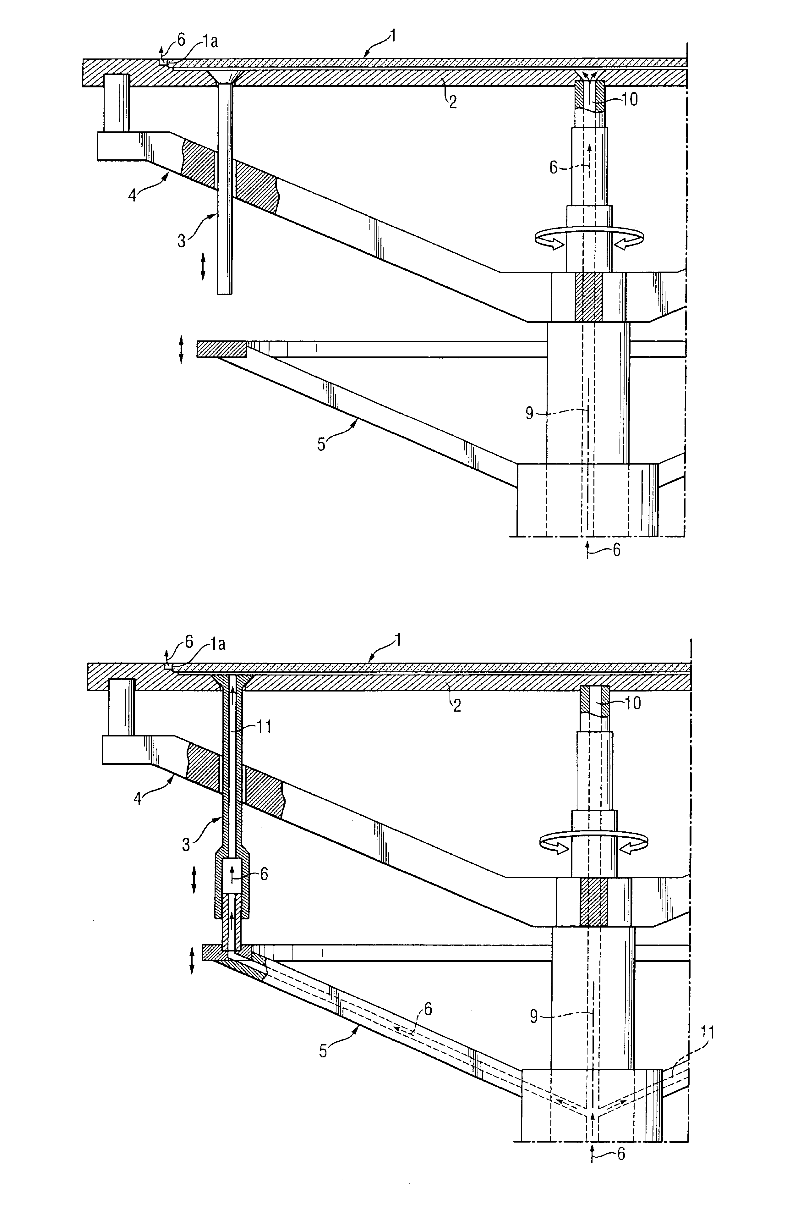
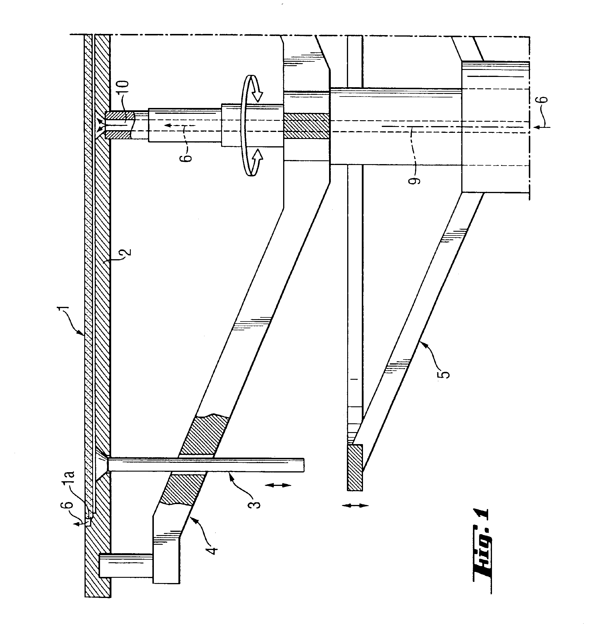
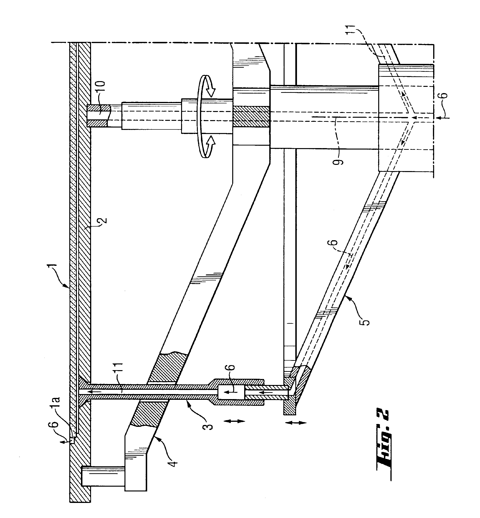
[0056]A silicon wafer with a diameter of 300 mm and a resistivity of 10 mΩcm was homoepitaxially coated in an epitaxy reactor at 1100° C. During the coating, the silicon wafer was rotated about its center axis at 32 revolutions per minute. The flow of hydrogen was 50 slm (standard liters per minute), the flow of trichlorosilane was 17 slm and the flow of diborane was 150 sccm (standard cubic centimeters per minute). Under these conditions, a 3 μm thick, boron-doped silicon layer with a resistivity of 5 Ωcm was deposited. According to the invention, argon was supplied during the epitaxial coating below the center of the silicon wafer, as shown in FIG. 1. The radius of, the feed was 1 cm. The recess in the susceptor (pocket) was designed in such a way that the distance between wafer back surface and the lowest point of the susceptor was 0.5 mm. The argon flowed in below the silicon wafer at a volumetric flow rate of 180 sccm. Under these conditions, a radial resistance variation on th...


PUM

PropertyMeasurementUnit
resistivityaaaaaaaaaa

Abstract

A process for epitaxially coating the front surface of a semiconductor wafer in a CVD reactor, the front surface of the semiconductor wafer being exposed to a process gas which contains a source gas and a carrier gas, and the back surface of the semiconductor wafer being exposed to a displacement gas, wherein the displacement gas contains no more than 5% by volume of hydrogen, with the result that diffusion of dopants out of the back surface of the semiconductor wafer, which is intensified by hydrogen, is substantially avoided. With this process, it is possible to produce a semiconductor wafer with a substrate resistivity of ≦100 mΩcm and a resistivity of the epitaxial layer of >1 Ωcm without back-surface coating, the epitaxial layer of which semiconductor wafer has a resistance inhomogeneity of <10%.

Description

BACKGROUND OF THE INVENTION[0001]1. Field of the Invention[0002]The present invention relates to a process and an apparatus for epitaxially coating a semiconductor wafer, and to an epitaxially coated semiconductor wafer.[0003]2. The Prior Art[0004]In semiconductor technology, crystal growth from the vapor phase is used in particular to produce epitaxially coated semiconductor wafers. The term epitaxy is understood as meaning the growth of a single-crystalline layer onto the planar boundary surface of a single-crystalline substrate, generally a substrate wafer, for example a semiconductor wafer. This coating or deposition takes place by means of what is known as chemical vapor deposition (CVD) in CVD reactors, as described for example in EP 714 998 A2. The semiconductor wafer is first of all heated by means of heating sources and then exposed to a gas mixture, referred to below as the process gas, comprising a source gas, a carrier gas and if appropriate a doping gas.[0005]One of the...

Claims


Application Information

Patent Timeline
Patent Type & Authority Patents(United States)
IPC IPC(8): C30B23/02H01L21/02H01L21/22C23C16/44H01L21/205
CPCC30B23/02C30B29/40H01L21/2205Y10T117/10Y10S438/913Y10S438/98Y10S438/928H01L21/20
Inventor VON AMMON, WILFRIEDSCHMOLKE, RUEDIGERSTORCK, PETERSIEBERT, WOLFGANG
Owner SILTRONIC AG
Why Eureka
Try Eureka