Dielectric film

a technology of dielectric film and film, applied in the field of dielectric film, can solve the problems of constant decrease of amount, inability to implement integrated electronics or electric fields in the early system, and short supply of sample quantities and volumes

Inactive Publication Date: 2005-05-10
ADVION
View PDF15 Cites 1 Cited by
  • Summary
  • Abstract
  • Description
  • Claims
  • Application Information

AI Technical Summary

Benefits of technology

[0015]Other advantages of the present invention will be apparent to those skilled in the art from the following description and the appended claims.

Problems solved by technology

However, due to the nature and origin of the materials under analysis, sample amounts and volumes are historically in short supply and these amounts are constantly decreasing.
None of the early systems implemented integrated electronics or electric fields for operation, but rather the silicon was used as a substrate for micromachining desired shapes / geometry.
The need for the ability to apply electric fields to the device becomes a serious issue when processing samples contained in the liquid phase on silicon substrates.
A difficult scenario is encountered due to the opposing objectives of the micro total analysis system and the microprocessor technology used to make them.
Typically, the microprocessor industry strives to keep microdevices “dry” and “clean” as liquids, moisture, and contaminates interfere with the device performance and operation.
However, major issues arise when electronics are incorporated in the devices and especially when potentials are applied for the generation of electric fields (semiconductor must be insulated for controlled electric field generation).
Additionally, the microprocessor industry has gone to great lengths to avoid contact of the electronic device with mobile ions such as salts due to the destructive nature they pose to dielectric coatings used to insulate the silicon used in microprocessors.
Application of high voltages to liquids on insulators on conductor substrates often leads to shorting or drastically reduced performance and lifetime of desired electrical properties.
The art lacks the ability to incorporate microfluidics and electronics in the same substrate allowing for fully integrated systems.

Method used


Image

  • Dielectric film
  • Dielectric film
  • Dielectric film

Examples


example 1

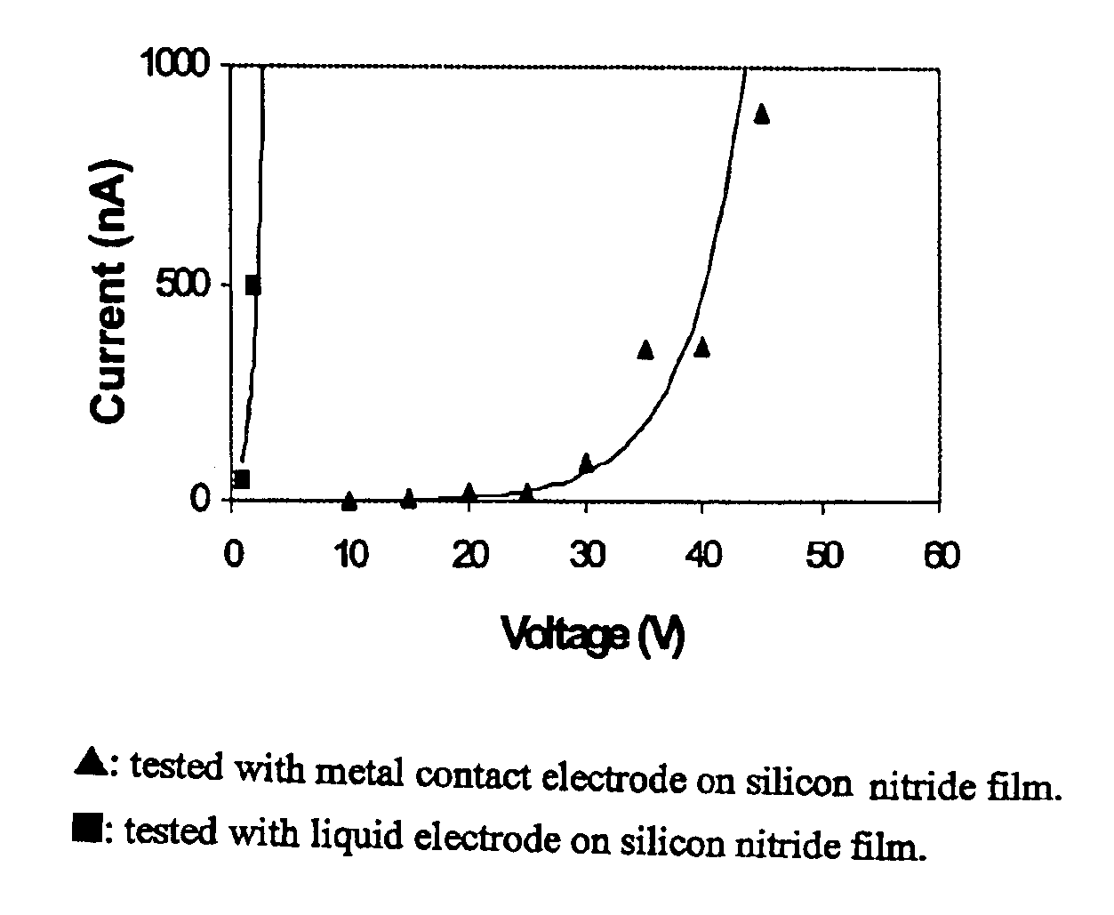
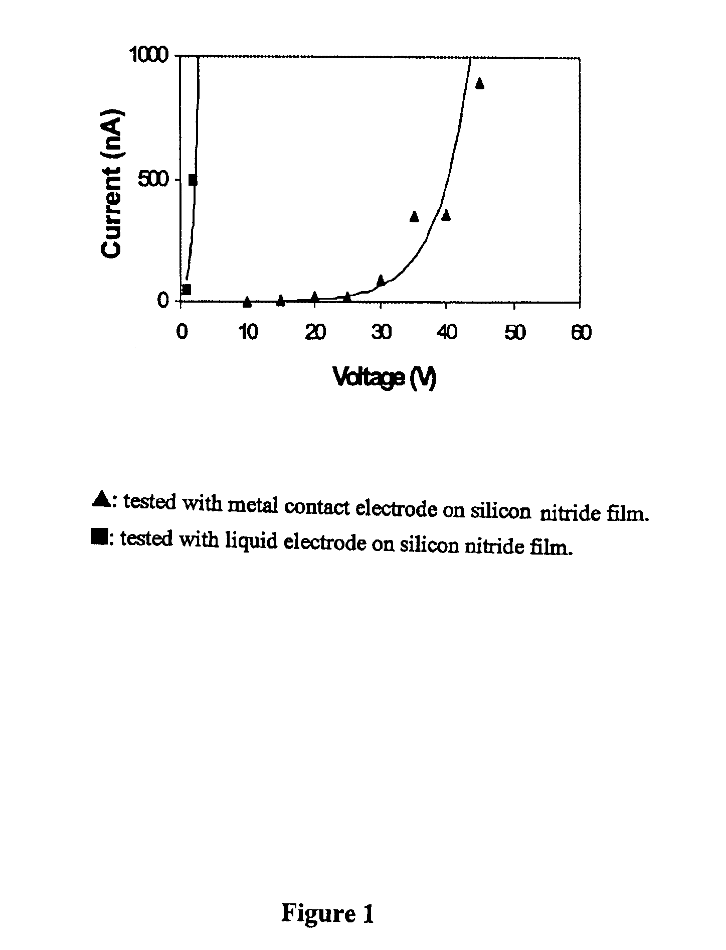
[0053]Data for FIG. 1 was generated using the following experimental setup and conditions. A silicon wafer was cleaned using semiconductor cleaning protocols (MOS clean). 100 nm low stress nitride was deposited on a silicon wafer in a low-pressure chemical vapor deposition oven. The sample was then cleaved and placed in an electrical test apparatus for assessment of the dielectric breakdown strength of the thin film. Conductive epoxy was used to make good electrical contact between the silicon substrate (cleaved edge of the wafer) and the grounded metal stage. Positive (or negative) voltage was applied under dry conditions using a metal electrode, or under wet conditions, utilizing a fluid electrode. The voltage was ramped up in a stepwise fashion while simultaneously monitoring the current leaking through the film to the silicon substrate. The curve was recorded and the data can be seen in FIG. 1. It is seen from this data that the current—voltage characteristics of the low stress ...

example 2

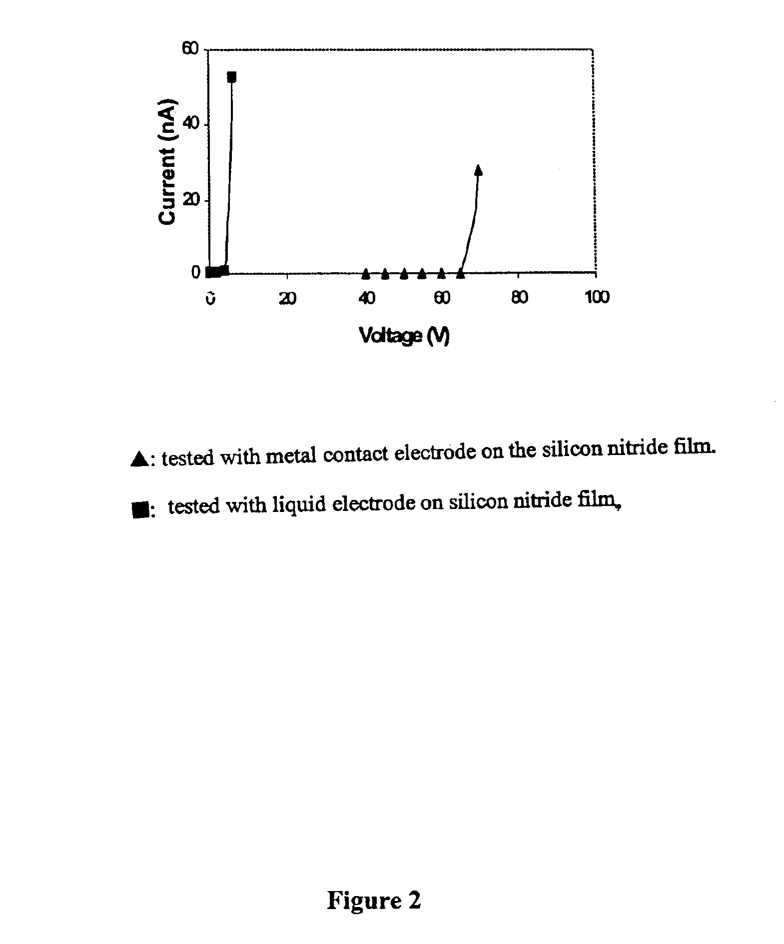
[0054]Data for FIG. 2 was generated using the following experimental setup and conditions. A silicon wafer was cleaned using semiconductor cleaning protocols (MOS clean). 100nm of high stress nitride was deposited on a silicon wafer in a low-pressure chemical vapor deposition oven. The sample was then cleaved and placed in an electrical test apparatus for assessment of the dielectric breakdown strength of the thin film. Conductive epoxy was used to make good electrical contact between the silicon substrate (cleaved edge of the wafer) and the grounded metal stage. Positive (or negative) voltage was applied under dry conditions using a metal electrode, or under wet conditions, utilizing a fluid electrode. The voltage was ramped up in a stepwise fashion while simultaneously monitoring the current leaking through the film to the silicon substrate. The curve was recorded and the data can be seen in FIG. 2. It is seen from this data that the nitride film has much less dielectric strength ...

example 3

[0055]Data for FIG. 3 was generated using the following experimental setup and conditions. A silicon wafer was cleaned using semiconductor cleaning protocols (MOS clean). 1.5 μm of low stress nitride was deposited on a silicon wafer in a low-pressure chemical vapor deposition oven. The wafer was then cleaved and one pieces was preserved for electrical testing with only the low stress nitride and another piece was further processed with the addition of a subsequent deposition of 100 nm of oxynitride. The samples were then cleaved and placed in an electrical test apparatus for assessment of the dielectric breakdown strength of the thin film. Conductive epoxy was used to make good electrical contact between the silicon substrates (cleaved edges of the wafer) and the grounded metal stage. Positive (or negative) voltage was applied under dry conditions using a metal electrode, or under wet conditions, utilizing a fluid electrode for both samples. The voltage was ramped up in a stepwise f...


PUM

PropertyMeasurementUnit
sizeaaaaaaaaaa
thickaaaaaaaaaa
dielectric strengthaaaaaaaaaa

Abstract

A dielectric film is provided which includes a base layer and a capping layer, preferably silicon oxynitride, wherein the film is an effective moisture and ion barrier when disposed between a conductive substrate and a liquid having an electrical potential different than the electrical potential of the substrate.

Description

[0001]This application claims the benefit of U.S. Provisional Patent Application Ser. No. 60 / 322,862, filed Sep. 17, 2001, which is herein incorporated by reference in its entirety.FIELD OF THE INVENTION[0002]The invention relates to a dielectric film and its use as a coating and insulation layer for liquids on electrically conductive materials. In particular, the invention relates to dielectric film and its use as a coating and insulating layer of a device, including microfluidic devices requiring electrical insulation and electrospray devices.BACKGROUND OF THE INVENTION[0003]The area of miniaturized microfluidic technology, also known as “lab-on-a-chip” or “micro total analysis systems”, is rapidly expanding with the promise of revolutionizing chemical analysis and offering enabling tools and technologies for the life sciences. The majority of molecules and compounds of interest in the life sciences are in the liquid phase and typically analytical measurements are used to conduct ...

Claims


Application Information

Patent Timeline
Patent Type & Authority Patents(United States)
IPC IPC(8): H01J49/02H01L29/76H01J49/04H01L29/66B32B7/00B81B1/00G01N27/447G01N30/72G01N37/00G02B1/11H01B3/10H01B3/12H01B7/282H01B17/60H01L21/306H01L29/00H01L29/74H01L29/78
CPCG01N27/44704H01B3/10H01B7/2825H01L21/3143H01L21/3145H01B3/12G01N30/7266H01L21/3146H01L21/0214H01L21/02164H01L21/02175H01L21/02115H01L21/02282H01L21/022H01L21/02271H01L21/02211H01L21/0217
Inventor LI, JIECORSO, THOMAS N.SCHULTZ, GARY A.
Owner ADVION
Why Eureka
Try Eureka