Barrier layer for a copper metallization layer including a low-k dielectric

a barrier layer and copper metallization technology, applied in the direction of semiconductor devices, semiconductor/solid-state device details, electrical apparatus, etc., can solve the problems of aluminum with copper not providing the required decrease of parasitic rc time constants, limiting device performance, signal propagation delay caused, etc., to reduce nitrogen concentration, reduce the diffusion barrier component through the second surface, and reduce the nitrogen concentration

Inactive Publication Date: 2005-05-17
ADVANCED MICRO DEVICES INC
View PDF20 Cites 20 Cited by
  • Summary
  • Abstract
  • Description
  • Claims
  • Application Information

AI Technical Summary

Benefits of technology

[0017]Generally, the present invention is directed to a semiconductor device and a method that provides the required nitrogen concentration at a lower portion of a dielectric barrier / etch stop layer so as to provide for the advantageous electromigration behavior of an adjacent copper material, while an upper portion of the barrier / etch stop layer has a significantly reduced nitrogen concentration, wherein in some embodiments an upper surface of the etch stop layer may be substantially completely depleted from nitrogen.

Problems solved by technology

In integrated circuits having minimum dimensions of approximately 0.35 μm and less, a limiting factor of device performance is the signal propagation delay caused by the switching speed of the transistor elements.
As the channel length of these transistor elements has now reached 0.18 μm and less, it turns out, however, that the signal propagation delay is no longer limited by the field effect transistors, but is limited, owing to the increased circuit density, by the close proximity of the interconnect lines, since the line-to-line capacitance is increased in combination with a reduced conductivity of the lines due to their reduced cross-sectional area.
For devices having feature sizes of 0.13 μm and less, it turns out that simply replacing aluminum with copper does not provide the required decrease of the parasitic RC time constants, and, therefore, the well-established and well-known dielectric materials, silicon dioxide (k approximately 4.2) and silicon nitride (k>5), are increasingly replaced by so-called low-k dielectric materials.
However, the transition from the well-known and well-established aluminum / silicon dioxide metallization layer to a low-k dielectric / copper metallization layer is associated with a plurality of issues to be dealt with.
For example, copper may not be deposited in higher amounts in an efficient manner by well-established deposition methods, such as chemical and physical vapor deposition.
Moreover, copper may not be efficiently patterned by well-established anisotropic etch processes; therefore, the so-called damascene technique is employed in forming metallization layers including copper lines.
Although silicon nitride is known as an effective copper diffusion barrier, silicon nitride may not be considered appropriate in low-k dielectric layer stacks owing to its high permittivity.
A further problem in forming low-k copper metallization layers has been under-estimated in the past and is now considered a major challenge in the integration of low-k dielectrics.
In developing the photoresist, certain portions of the resist which have been exposed may not be completely removed as required and thus the structure may not be correctly transferred into the underlying low-k dielectric material.
The interaction of nitrogen and compounds thereof with the photoresist may deteriorate the light sensitivity of the resist.
It turns out, however, that even the provision of a photoresist bi-layer is insufficient in preventing resist poisoning.
Moreover, even a significant increase of the thickness of the anti-reflective coating 112 may not efficiently prevent the overlying photoresist layer 113 from interacting with up-diffusing nitrogen-containing compounds.
However, since the trenches 117 required for the electrical connection are missing, as shown in FIGS. 1d and 1e, or are at least substantially reduced in size, device failures consequently occur or at least a significantly reduced device reliability is obtained.

Method used


Image

  • Barrier layer for a copper metallization layer including a low-k dielectric
  • Barrier layer for a copper metallization layer including a low-k dielectric
  • Barrier layer for a copper metallization layer including a low-k dielectric

Examples


Embodiment Construction

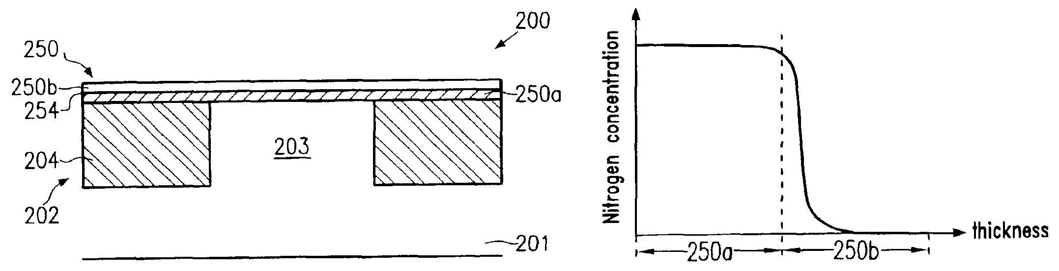
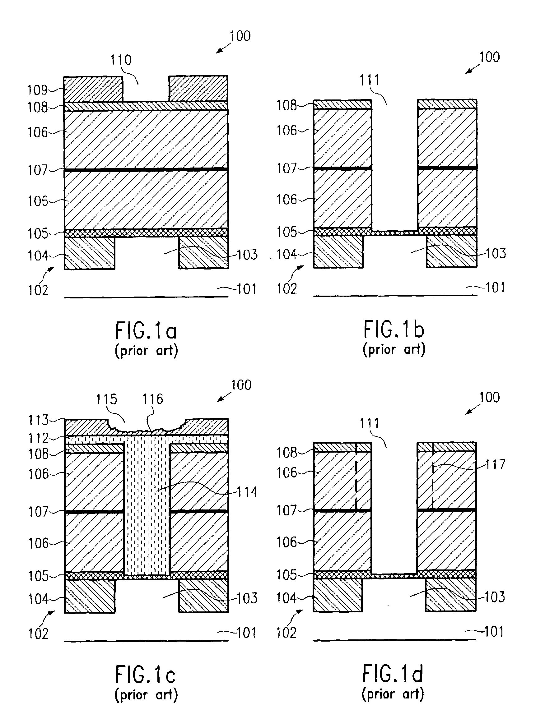
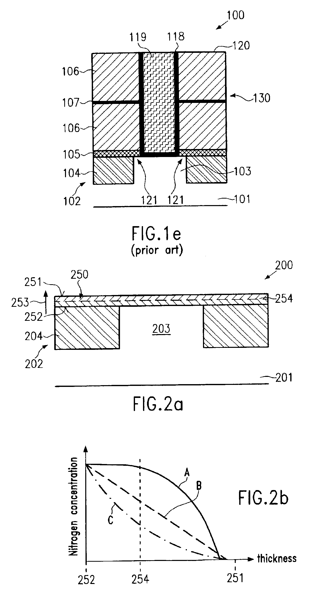
[0030]Illustrative embodiments of the invention are described below. In the interest of clarity, not all features of an actual implementation are described in this specification. It will of course be appreciated that in the development of any such actual embodiment, numerous implementation-specific decisions must be made to achieve the developers' specific goals, such as compliance with system-related and business-related constraints, which will vary from one implementation to another. Moreover, it will be appreciated that such a development effort might be complex and time-consuming, but would nevertheless be a routine undertaking for those of ordinary skill in the art having the benefit of this disclosure.

[0031]The present invention will now be described with reference to the attached figures. Although the various regions and structures of a semiconductor device are depicted in the drawings as having very precise, sharp configurations and profiles, those skilled in the art recogni...


PUM


Abstract

The effect of resist poisoning may be eliminated or at least substantially reduced in the formation of a low-k metallization layer, in that a nitrogen-containing barrier / etch stop layer is provided with a significantly reduced nitrogen concentration at an interface in contact with said low-k dielectric material. Consequently, diffusion of nitrogen and nitrogen compounds in vias formed in said low-k dielectric layer is significantly suppressed, so that in a subsequent photolithographic step, interaction of nitrogen and nitrogen compounds with the photoresist is remarkably reduced.

Description

BACKGROUND OF THE INVENTION[0001]1. Field of the Invention[0002]Generally, the present invention relates to the formation of integrated circuits, and, more particularly, to the formation of metallization layers including highly conductive metals, such as copper, embedded into a dielectric material having low permittivity to enhance device performance.[0003]2. Description of the Related Art[0004]In modern integrated circuits, minimum feature sizes, such as the channel length of field effect transistors, have reached the deep sub-micron range, thereby steadily increasing performance of these circuits in terms of speed and power consumption. As the size of the individual circuit elements is significantly reduced, thereby improving, for example, the switching speed of the transistor elements, the available floor space for interconnect lines electrically connecting the individual circuit elements is also decreased. Consequently, the dimensions of these interconnect lines have to be reduc...

Claims


Application Information

Patent Timeline
Patent Type & Authority Patents(United States)
IPC IPC(8): H01L23/52H01L21/70H01L23/532H01L21/768
CPCH01L21/76801H01L21/76808H01L21/76822H01L23/53295H01L21/76834H01L21/76826H01L23/53238H01L2924/0002H01L2924/00
Inventor RUELKE, HARTMUTHOHAGE, JOERGWERNER, THOMASAMINPUR, MASSUD
Owner ADVANCED MICRO DEVICES INC
Why Eureka
Try Eureka