Electrophotographic photoconductor, electrophotographic apparatus and process cartridge

a photoconductor and electrophotography technology, applied in the direction of electrographic process apparatus, instruments, corona discharge, etc., can solve the problems of incompatibility with higher durability, decrease of optical transmittance and image deterioration, and strength decline, so as to improve wear resistance, reduce foreign matter adhesion, and improve image quality

Inactive Publication Date: 2005-05-31
RICOH KK
View PDF8 Cites 63 Cited by
  • Summary
  • Abstract
  • Description
  • Claims
  • Application Information

AI Technical Summary

Benefits of technology

[0020]It is therefore an object of the present invention, which was conceived in view of the above problems, to inhibit blurred or other image defects by improving wear resistance and lessening adhesion of foreign matter to a photoconductor surface, to realize high image quality by improving transfer efficiency and cleaning properties, and by enhancing the continuation of these effects, to provide an electrophotographic photoconductor having improved image stability, together with an electrophotographic apparatus and electrophotographic cartridge using this photoconductor.

Problems solved by technology

However, when the mold release properties are increased in a lubricant of the related art, this effect is not easily maintained, and wear resistance has to be sacrificed to enhance the effect, hence it is incompatible with higher durability.
Also, when the photoconductor is exposed to form an electrostatic latent image thereon, these lubricants tend to scatter the light which led to a decrease of optical transmittance and image deterioration.
The strength decreased, and the photoconductor has lower resistance to scratches, which lowered wear resistance and lead to cleaning defects.
Moreover, the addition of these lubricants causes a higher residual potential which adversely impacts image stability.
These lubricants, which are added to enhance mold release properties, by their very nature, cause a sharp drop of compatibility with the binder resin or organic solvents used in the photoconductor.
Therefore, in the case of microfine particle lubricants, clumps tends to form, leading to a further loss of optical transmittance and decrease of surface flatness of the photoconductor, as well as deterioration of layer quality.
As a result, there is not only less resistance to scratches and lower wear resistance, but unevenness occurs during charging, developing, transfer and cleaning.
This makes it impossible to increase durability, and also have a serious adverse impact on the suppression of image defects.
As these microfine particle lubricants are associated with many problems, as described above, a sufficient amount of them could not be added, so that foreign matter could not be sufficiently removed from the photoconductor surface, and higher durability could not be achieved.

Method used


Image

  • Electrophotographic photoconductor, electrophotographic apparatus and process cartridge
  • Electrophotographic photoconductor, electrophotographic apparatus and process cartridge
  • Electrophotographic photoconductor, electrophotographic apparatus and process cartridge

Examples


example 1

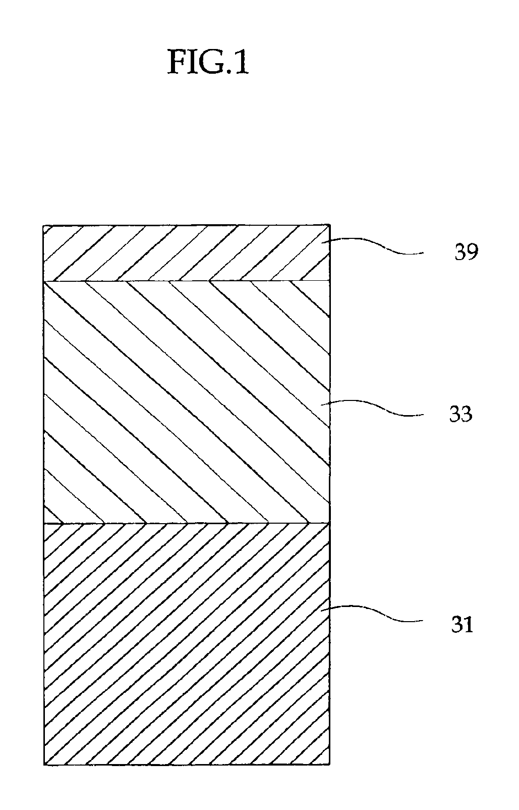
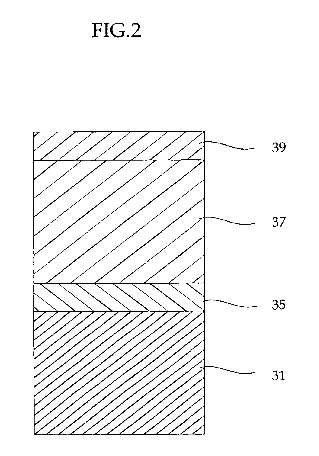
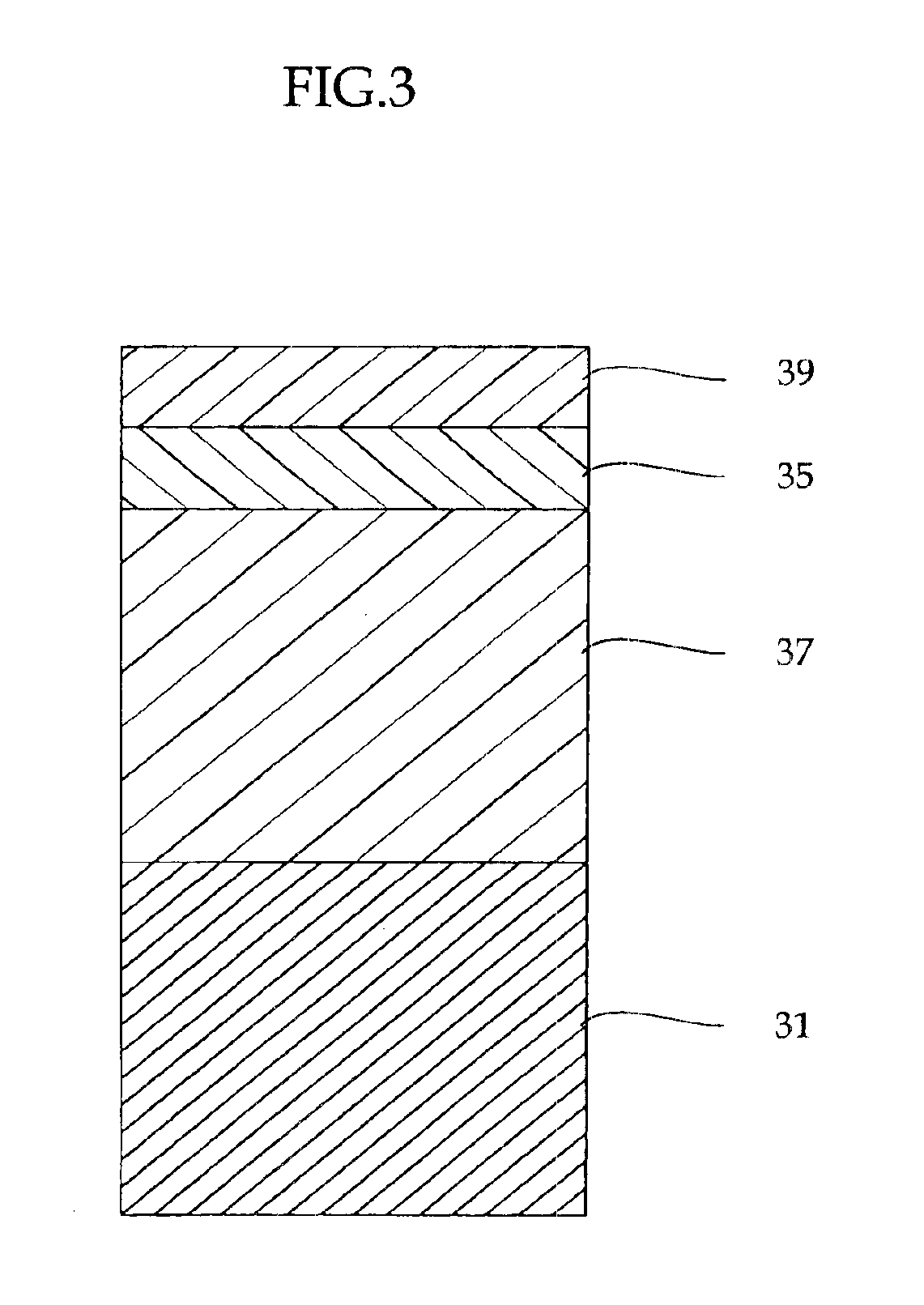
[0204]An underlayer of approximately 3.5 μm, a charge-generating layer of approximately 0.2 μm and a charge transport layer of approximately 20 μm were formed by impregnation coating method, in which an underlayer coating solution, a charge-generating layer coating solution and a charge transport layer coating solution having the following compositions, were sequentially applied on an aluminium drum of diameter 30 mm. A protective layer of approximately 5.0 μm was then formed by spray coating method, in which a protective layer coating solution was prepared as described below, and heated in an oven at 150° C. for 30 minutes so as to manufacture a photoconductor 1.

[Underlayer Coating Solution]

[0205]

Alkyde resin6parts(Bekozole 1307-60-EL, DAINIPPON INK ANDCHEMICALS, INCORPORATED)Melamine resin4parts(Super Bekamine G-821-60, DAINIPPON INK ANDCHEMICALS, INCORPORATED)Titanium oxide40partsMethyl ethyl ketone50parts[Charge-generating layer coating solution]Bis-azo pigment expressed by Form...

example 2

[0207]A photoconductor 2 was manufactured in the same way as in Example 1, except that the protective layer coating solution of Example 1 was changed to the following protective layer coating solution.

[Protective Layer Coating Solution]

[0208]6 parts of acryl-modified polyorganosiloxane (CHALINE R-170S, Nissin Chemical Industry Co., Ltd.), 15 parts of styrene-MMA (methyl methacrylate)-2-HEMA (hydroxyethyl methacrylate) copolymer (20% by weight 2-ethoxyethyl acetate / methylisobutyl ketone solution), 3 parts of a polymer having a charge transport function, expressed by Formula (ii), 30 parts of cellosolve acetate and 10 parts of methyl isobutyl ketone were mixed and dispersed by a ball mill for 120 hours. 40 parts of a mixed solution of hexamethylene diisocyanate-trimethylolpropane adduct, acetone and ethyl acetate, was then added, and stirred to prepare a coating solution.

example 3

[0209]A photoconductor 3 was manufactured in the same way as in Example 1, except that the protective layer coating solution of Example 1 was changed to the following protective layer coating solution.

[Protective Layer Coating Solution]

[0210]3 parts of acryl-modified polyorganosiloxane (CHALINE R-170S, Nissin Chemical Industry Co., Ltd.), 15 parts of MMA (methyl methacrylate)-BMA (butyl methacrylate)-HEMA (hydroxyethyl methacrylate) copolymer (50% by weight toluene / butyl acetate solution), 2 parts of α-alumina (Sumi Corundum AA-03, average first-order particle diameter: 0.3 μm, Sumitomo Chemical Industries), 0.05 parts of a polycarbonate compound (BYK-P104, 50% by weight xylene solution, BYK-Chemie Japan K.K.) and 20 parts of cyclohexanone were mixed and dispersed by a ball mill for 50 hours. A mixed solution of 5 parts benzoguanamine resin (80% by weight butyl cellosolve solution), 0.05 parts of an aromatic sulfonic acid (40% by weight isopropyl alcohol solution), 7 parts of a low ...


PUM

PropertyMeasurementUnit
order particle diameteraaaaaaaaaa
first-order particle diameteraaaaaaaaaa
particle diameteraaaaaaaaaa

Abstract

The present invention aims to provide a photoconductor having improved wear resistance, and which has reduced foreign matter attached on the photoconductor surface.
The electrophotographic photoconductor of the present invention is formed by sequentially disposing a photoconductive layer comprising at least one layer and a protective layer on an electroconductive support, and the protective layer comprises an acrylic resin and/or a methacrylic resin and a resin composition comprising an acryl-modified polyorganosiloxane compound which is dispersed in or compatible with the acrylic resin and/or the methacrylic resin.

Description

BACKGROUND OF THE INVENTION[0001]1. Field of the Invention[0002]The present invention relates to an electrophotographic photoconductor which has high durability, high image quality and improved image stability over a long period of time, to an electrophotographic apparatus using the same, and to a process cartridge using the same.[0003]2. Description of the Related Art[0004]In an electrophotographic apparatus using the electrophotography method, such as a copying machine, facsimile, laser printer or direct digital machine, a toner image is formed on an electrophotographic photoconductor (also referred as photoconductor, hereinafter), mainly by charging, irradiating light imagewisely so as to form a latent electrostatic image and developing the latent electrostatic image. Thereafter, the toner image is transferred to a transfer medium such as a piece of paper, and then fixed on the paper. Further, the residual toner and the like on the surface of the photoconductor are removed so as ...

Claims


Application Information

Patent Timeline
Patent Type & Authority Patents(United States)
IPC IPC(8): G03G5/05G03G5/147
CPCG03G5/0557G03G5/0578G03G5/14791G03G5/14717G03G5/14747G03G5/0592
Inventor TAMOTO, NOZOMUSUZUKI, YASUONAGAI, KAZUKIYOLI, HONGGUO
Owner RICOH KK
Why Eureka
Try Eureka