Film bulk acoustic resonator

a resonator and bulk technology, applied in the direction of bulk negative resistance effect devices, electrical equipment, semiconductor devices, etc., can solve the problem that the performance of thin film resonators or thin film band-pass filters which cannot meet the giga-hertz band has not been obtained, and achieves high crystallinity, convenient growth, and superior characteristics.

Inactive Publication Date: 2005-08-30
NAT INST OF ADVANCED IND SCI & TECH +1
View PDF17 Cites 87 Cited by
  • Summary
  • Abstract
  • Description
  • Claims
  • Application Information

AI Technical Summary

Benefits of technology

[0013]The present inventors have found that resonance characteristics of FBAR including an AlN thin film formed as a piezoelectric thin film (piezoelectric film) on a substrate of Si or the like are remarkably improved by adding a third component such as an alkaline earth metal, a rare earth metal and the like to the AlN thin film. It has also been found that with the use of a high-quality AlN thin film to which the third component has been added in FBAR, it is possible to realize a high-performance FBAR large in an electromechanical coupling coefficient and superior in a Q value, bandwidth and frequency-temperature characteristic, and the present invention has been reached.

Problems solved by technology

However, the thin film resonator or thin film band-pass filter which fulfils a sufficient performance in a giga-hertz band has not been obtained yet, and there has been a demand for improvement of an acoustic quality factor (Q value), temperature coefficient of frequency, and insertion loss of the AlN thin film.

Method used


Image

  • Film bulk acoustic resonator
  • Film bulk acoustic resonator
  • Film bulk acoustic resonator

Examples


example 1

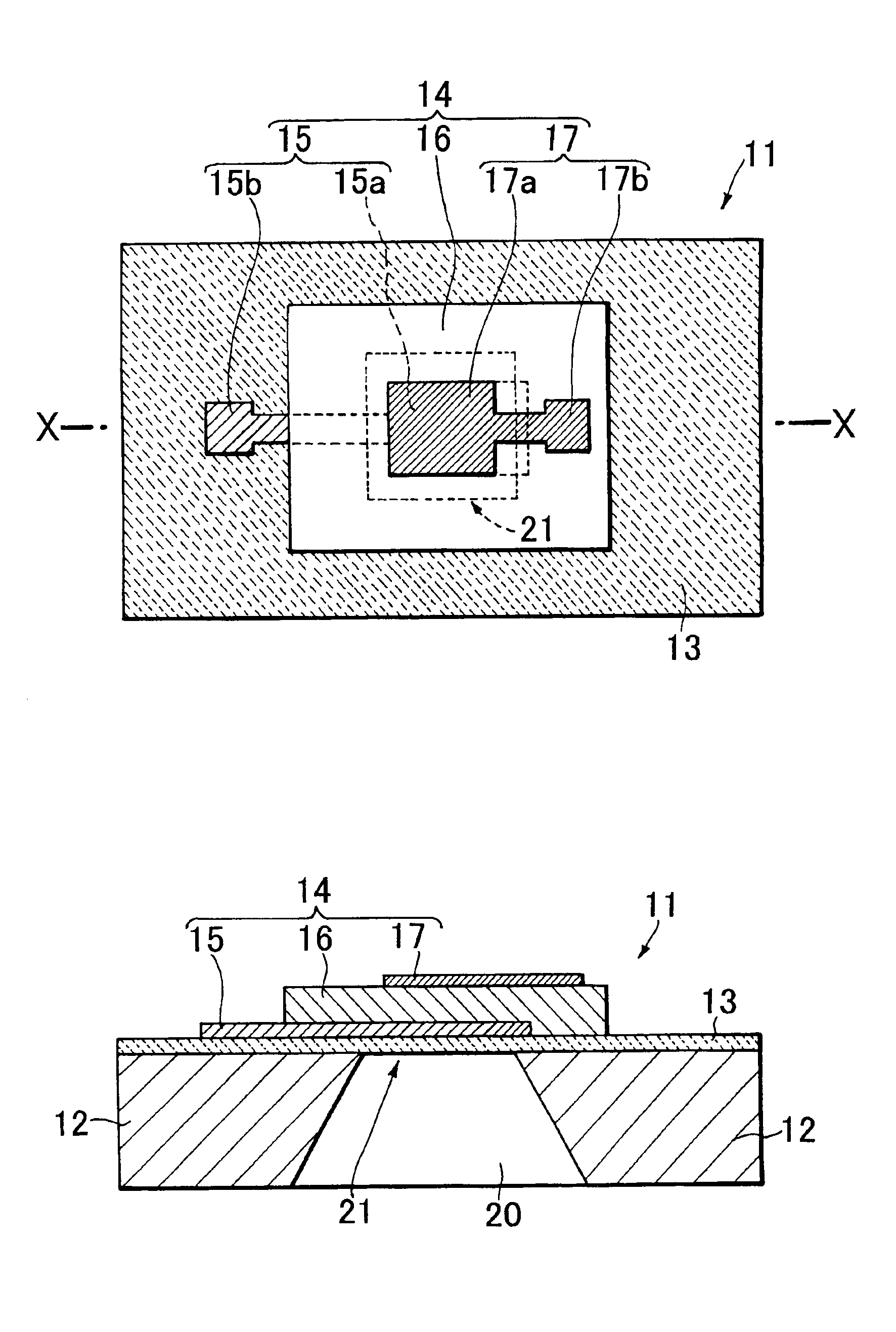
[0120]In the present example, the thin film bulk acoustic resonator having the structure shown in FIGS. 1, 2 was prepared as follows.

[0121]That is, a silicon nitride (SiNx) layer having a thickness of 0.55 μm was formed on the upper and lower surfaces of the (100) Si substrate 12 having a thickness of 250 μm by a low-pressure CVD method. The SiNx layer on the upper surface was formed as the base film 13. Moreover, the SiNx layer on the lower surface was formed in a pattern of a mask for forming the via hole described later with respect to the substrate 12.

[0122]A Mo layer having a thickness of 200 nm was formed on the surface of the base film 13 by a DC magnetron sputtering method, and patterned by photolithography to form the lower electrode 15. The main portion 15a of the lower electrode 15 was formed in the shape close to a rectangular shape having a plane dimension of 140×160 μm. It was confirmed by X-ray diffraction measurement that the lower electrode 15 was the single orienta...

examples 2 to 4

[0126]In each of the present examples, the thin film bulk acoustic resonator having the structure shown in FIGS. 1, 2 was prepared as follows.

[0127]That is, a silicon oxide (SiO2) layer having a thickness in a range of 0.2 to 0.7 μm was formed on the upper and lower surfaces of the Si substrate 12 having a thickness of 300 μm by a thermal oxidation method. The SiO2 layer on the upper surface was formed as the base film 13. Moreover, the SiO2 layer on the lower surface was formed in the pattern of the mask for forming the via hole described later with respect to the substrate 12.

[0128]A stacked film of a 15 nm thick Ti layer and a 100 nm thick Pt layer on the Ti layer was formed on the surface of the base film 13 by the DC magnetron sputtering method, and patterned by the photolithography to form the lower electrode 15. The main portion 15a of the lower electrode 15 was formed in the shape close to the rectangular shape having a plane dimension of 140×160 μm. It was confirmed by the ...

examples 5

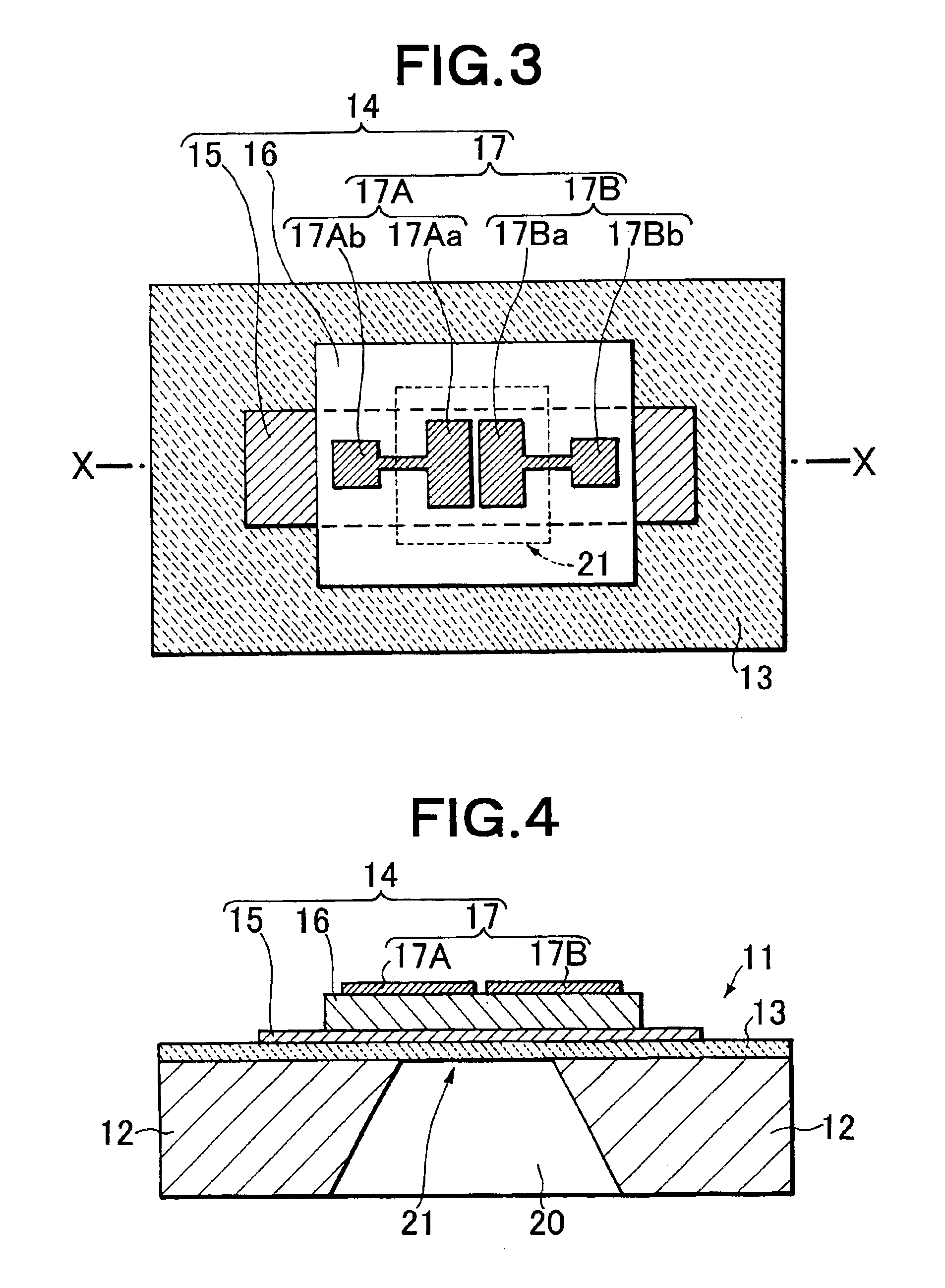
[0132]In the present example, the thin film bulk acoustic resonator having the structure shown in FIGS. 3, 4 was prepared as follows.

[0133]Steps similar to those of Example 1 were carried out except the shapes and dimensions of the upper and lower electrodes 15, 17. The lower electrode 15 was formed in the rectangular shape having a plane dimension of 120×280 μm so as to extend while including the region corresponding to the vibratory section 21. For the upper electrode 17, the main portions 17Aa, 17Ba each having the shape close to the rectangular shape having the plane dimension of 65×85 μm were arranged at an interval of 20 μm.

[0134]With respect to the thin film bulk acoustic resonator (FBAR) obtained in the above-described steps, the composition of the AlN piezoelectric film 16 was analyzed by the XPS spectroscopy. Moreover, the multifunctional X-ray diffraction apparatus for the surface structure evaluation was used to carry out the thin film X-ray diffraction measurement by th...


PUM


Abstract

A thin film bulk acoustic resonator comprises a substrate (12) of a silicon single crystal, a base film (13) formed on the substrate (12) and composed of a dielectric film mainly containing silicon oxide, and a piezoelectric stacked structure (14) formed on the base film (13). A vibratory section (21) composed of a part of the base film (13) and a part of the piezoelectric stacked structure (14). The piezoelectric stacked structure (14) includes a lower electrode (15), a piezoelectric film (16), and an upper electrode (17) formed in this order from below. The substrate (12) had a via hole (20) in the region corresponding to the vibratory section (21). The via hole forms a space for allowing vibration of the vibratory section (21). The piezoelectric film (16) is an aluminum nitride thin film containing 0.2 to 3.0 atom % of alkaline earth metal and / or a rare earth metal. Thus, the thin film bulk acoustic resonator has a high performance such as a large electromechanical coupling coefficient, an excellent acoustic quality factor (Q) and an excellent frequency-temperature characteristic.

Description

[0001]This application is a 371 of PCT / JP02 / 04576 filed on May 10, 2002, published on Nov. 21, 2002 under publication number WO 02 / 093740 A1 and claims priority benefits of Japanese Patent Application No. 2001-141846 filed May 11, 2001 and Japanese Patent Application No. 2001-182196 filed Jun. 15, 2001 and Japanese Patent Application No. 2001-394388 filed Dec. 26, 2001.TECHNICAL FIELD[0002]The present invention relates to a thin film bulk acoustic resonator which is a device using a piezoelectric thin film for use in a broad field such as a thin film resonator, a thin film voltage controlled oscillator (VCO), a thin film band-pass filter, a duplexer, various types of sensors, and the like used in mobile communication equipments, and the like.[0003]Moreover, the present invention relates to a stacked structure using an aluminum nitride thin film useful as a piezoelectric thin film of the thin film bulk acoustic resonator.BACKGROUND ART[0004]A device based on a piezoelectric phenomeno...

Claims


Application Information

Patent Timeline
Patent Type & Authority Patents(United States)
IPC IPC(8): H03H9/00H03H9/56H03H9/02H03H9/58
CPCH03H9/02094H03H9/174H03H9/562H03H9/564H03H9/585H03H9/588Y10S438/90H03H9/24
Inventor YAMADA, TETSUONAGAO, KEIGOHASHIMOTO, CHISENAKIYAMA, MORITOUENO, NAOHIROTATEYAMA, HIROSHI
Owner NAT INST OF ADVANCED IND SCI & TECH
Why Eureka
Try Eureka