

Nano-size semiconductor component and method of making
a semiconductor and nano-size technology, applied in nanoinformatics, enzymology, drug compositions, etc., can solve the problems of poor reproducibility of passivation process, increased resistivity, and metal compatibility difficulties with high thermal conductivity ceramic materials such as aln and si
- Summary
- Abstract
- Description
- Claims
- Application Information
AI Technical Summary
Benefits of technology
Problems solved by technology
Method used
Image

Examples
example i
Fabricating a Nanoconductor in a Semiconductor
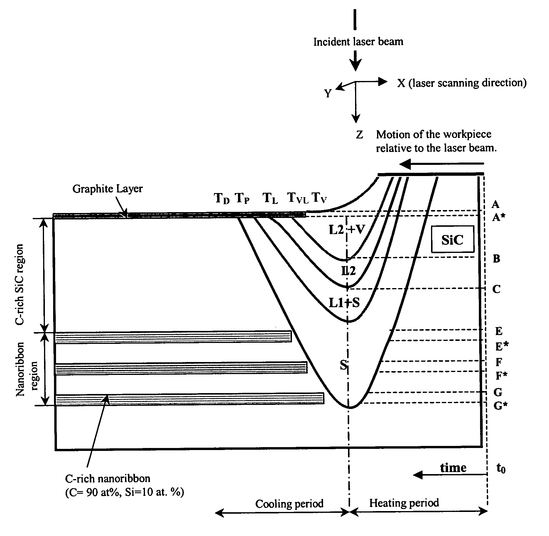
[0083]A 4H-Silicon Carbide single crystal substrate was irradiated with Nd:YAG, 1064 nm wavelength emisson, having a 260 ns pulse width, 35 kHz pulse repetition rate Q-switched laser, using an optimal power of 69.3 W. The 4H-Silicon Carbide single crystal substrate was positioned in an air-tight chamber with an atmosphere of Nitrogen gas. The laser beam was transmitted through a soda-lime glass window. Beam scanning was achieved either by a galvo-mirror or an x-y programmable table. The beam diameter was 1.0 mm and the beam scan speed 5.0 mm / sec. Nanoribbon conductors having a nano-polycrystalline structure, as analyzed by high resolution transmission electron microscopy (Techni F30) using selected area electron diffraction (SAED) after focussed in beam milling, were formed within the substrate using an optimal intensity of 8820 W / cm2 in a nitrogen environment. The heating rate and cooling rate was approximately a factor of 10 (an order ...
example ii
Theoretical
Fabricating a Nanoconductor in a Semiconductor
[0085]A 4H—SiC single crystal substrate was irradiated with an electron-gun beam (Tectra e-flux, Germany) operated at 300 KV and 200 mA producing 600 W. The 4H-Silicon Carbide single crystal substrate was positioned in a vacuum chamber with the electron-gun. Exposure was either timed to simulate the interaction time created by a 5 mm / sec beam scan speed or was achieved by an x-y programmable table). The beam diameter was estimated to be 2 mm diameter. The nano-ribbon conductors having a nano-polycrystalline structure, as analyzed by high resolution transmission electron microscopy (Techni F30) using selected area electron diffraction (SAED) after focused ion beam milling, were formed within the substrate using an intensity of 19,100 W / cm2 in vacuum. The process conditions resulted in an electron beam-material interaction time greater than 0.01 sec. The nano-ribbon conductors formed a heterostructure having a carbon atomic % ra...
example iii
Theoretical
Fabricating Nanoconductors in a Semiconductor Substrate to Create Internal Conductors and Devices and Sensors
[0091]A semiconductor silicon carbide single crystal substrate was irradiated with Nd:YAG, 1064 nm wavelength emission, having a 260 ns pulse width, 35 kHz pulse repetition rate Q-switched laser, using an optimal power of 69.3 W. The semiconductor silicon carbide single crystal substrate was positioned in an air-tight chamber with an atmosphere of nitrogen gas. The laser beam was transmitted through a soda-lime glass window. Beam scanning was achieved either by galvo-mirror or an x-y programmable table. The beam diameter was 1.0 mm and the beam scan speed 5.0 mm / s. The beam was focused on the substrate surface or at a depth within the surface. Nanoribbon conductors having a nano-polycrystalline structure, as analyzed by high resolution transmission electron microscopy (Techni F30) using selected area electron diffraction (SAED) after focussed ion beam milling, were...
PUM
 Abstract
Description
Claims
Application Information