

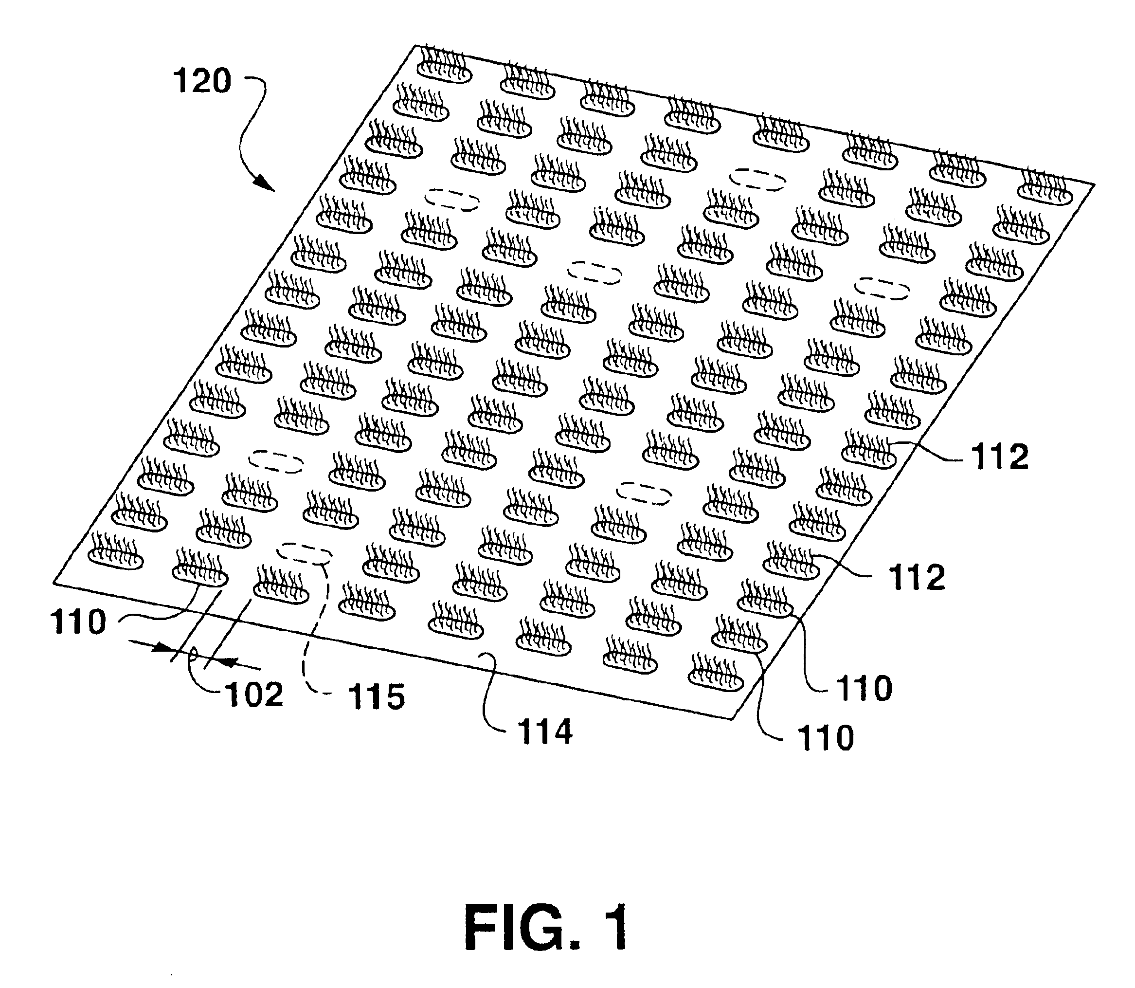
DNA-based memory device and method of reading and writing same
a memory device and dna technology, applied in the field of dna-based memory devices and methods of reading and writing same, can solve the problems of electronic noise, on-going development problem, physical limit to continuing reduction in the size of the structures which form electronics-based memory cells, etc., and achieve the effect of increasing the information storage density of the devi
- Summary
- Abstract
- Description
- Claims
- Application Information
AI Technical Summary
Benefits of technology
Problems solved by technology
Method used
Image

Examples
example 1
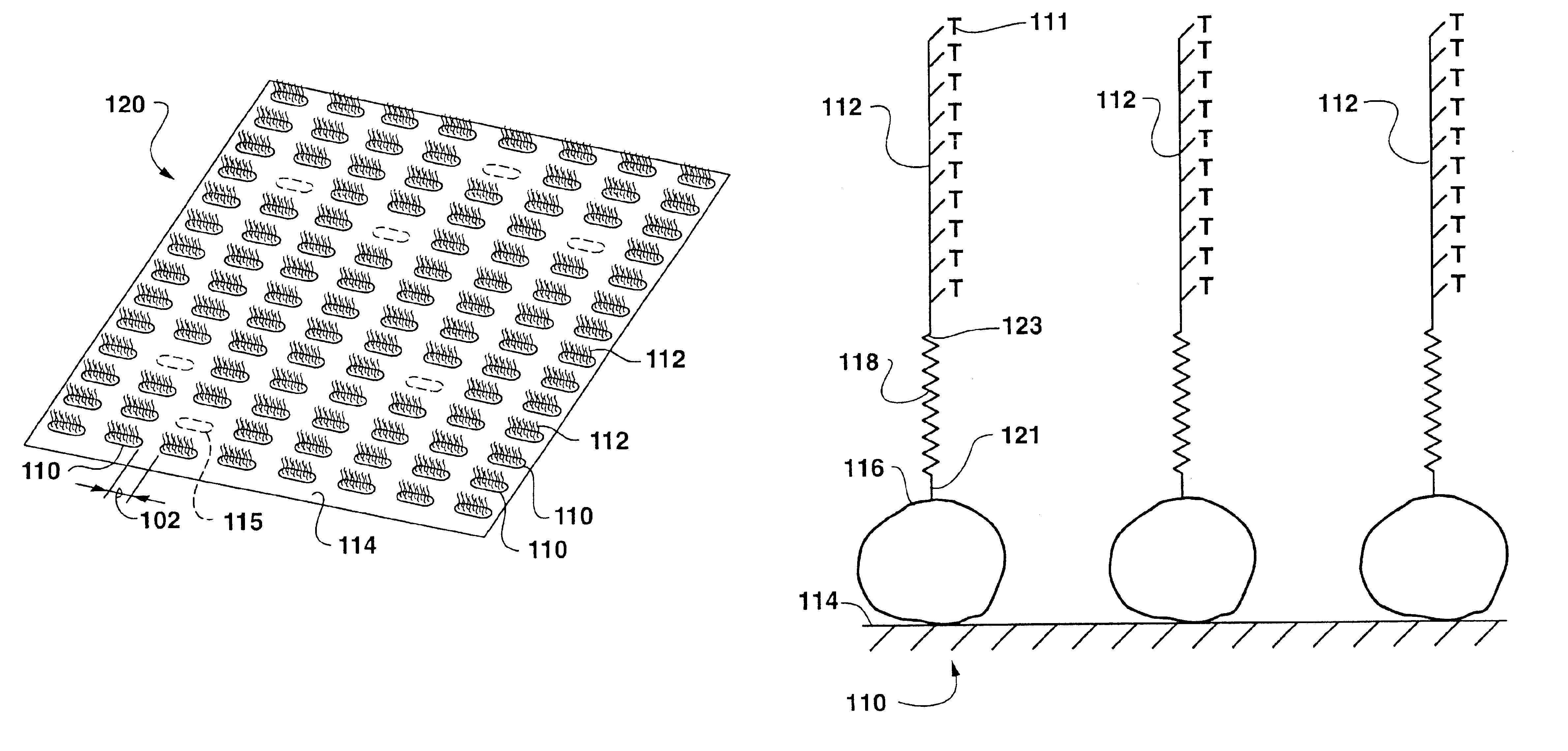
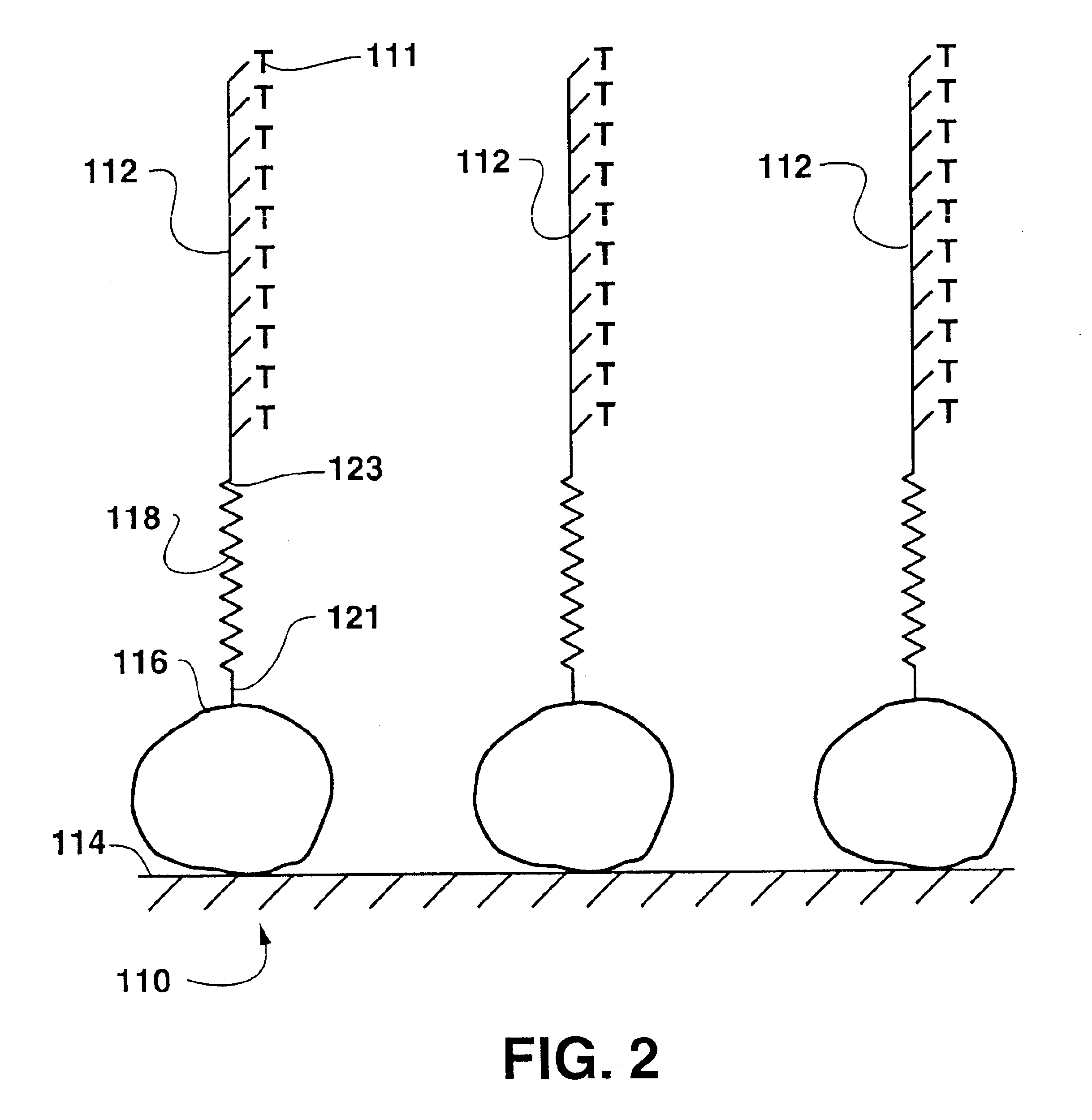
[0097]A portion of a thin slide of mica was coated with a layer of biotin labeled bovine serum albumin, followed by a coating with streptavidin to provide a surface upon which to array biotin labeled oligonucleotides. Five oligonucleotides were utilized in order to construct a memory device, Biotin-5′AAAAAAAAAA3′-Fluorescein (oligoA), Biotin-5′GGGGGGGGGG3′-Fluorescein (oligoG), Biotin-5′CCCCCCCCCC3′-Fluorescein (oligoC), Biotin-5′TTTTTTTTTT3′-Fluorescein (oligoT) and Biotin-5′AAAAAAAAAGGGGGGGGGG3′-Fluorescein (oligoAG). The slide served as the bottom surface of an empty AFM fluid cell. Microdrops of approximately 100 nl of the five oligonucleotides in buffer solution were placed upon the cover slip, in a region not coated with streptavidin. These microdrops served as a reference marker allowing re-positioning of each additional AFM tip as it was used. AFM silicon nitride pyramidal tips coated with biotin labeled bovine serum albumin, followed by a coating with streptavidin were util...
example 2
[0099]In this example, AFM was used to read the array of DNA code written in Example 1. Each of the four oligonucleotides oligo-A, oligo-G, oligo-C, and oligo-T, were affixed to an AFM tip and separately “dragged” along the linear stretches of the DNA chip array from Example 1. When oligo-A was so “dragged”, discrete interaction forces between the tip bound oligo-A and any oligo-T cells on the substrate were measured by cantilever deflection measured by AFM, providing evidence for the position of each T spot within the DNA chip array. Similar operations using the tips bearing oligo-G, oligo-T and oligo-C indicated the positions of the other three positions of the DNA chip array.
[0100]FIG. 8 shows the recorded AFM cantilever deflection curve shown as a function of force as the AFM arm was moved across the substrate and recognized the DNA code written on the chip. As the AFM tip passed over the memory cell which held the complementary DNA strand (between about 12 and about 15 nm on th...
PUM
| Property | Measurement | Unit |
|---|---|---|
| distance | aaaaa | aaaaa |
| distance | aaaaa | aaaaa |
| voltage | aaaaa | aaaaa |
Abstract
Description
Claims
Application Information