Semiconductor device including bipolar transistor and buried conductive region

Inactive Publication Date: 2005-09-13
MITSUBISHI ELECTRIC CORP
View PDF10 Cites 19 Cited by
  • Summary
  • Abstract
  • Description
  • Claims
  • Application Information

AI Technical Summary

Benefits of technology

[0010]An object of the present invention is to provide a semiconductor device and a manufacturing method for the same wherein a semiconductor substrate of a high resistance is used so that the Q value of the passive circuit elements can be enhan

Problems solved by technology

Therefore, it is difficult to form capacitors or inductors having Q values that are sufficiently large in high frequency regions by using an Si substrate.
In the case that a high resistance substrate, as described above, is used, however, the following problems arise.
Therefore, there is a risk that leakage current will increase from a collector region to the s

Method used


Image

  • Semiconductor device including bipolar transistor and buried conductive region
  • Semiconductor device including bipolar transistor and buried conductive region
  • Semiconductor device including bipolar transistor and buried conductive region

Examples


first embodiment

(First Embodiment)

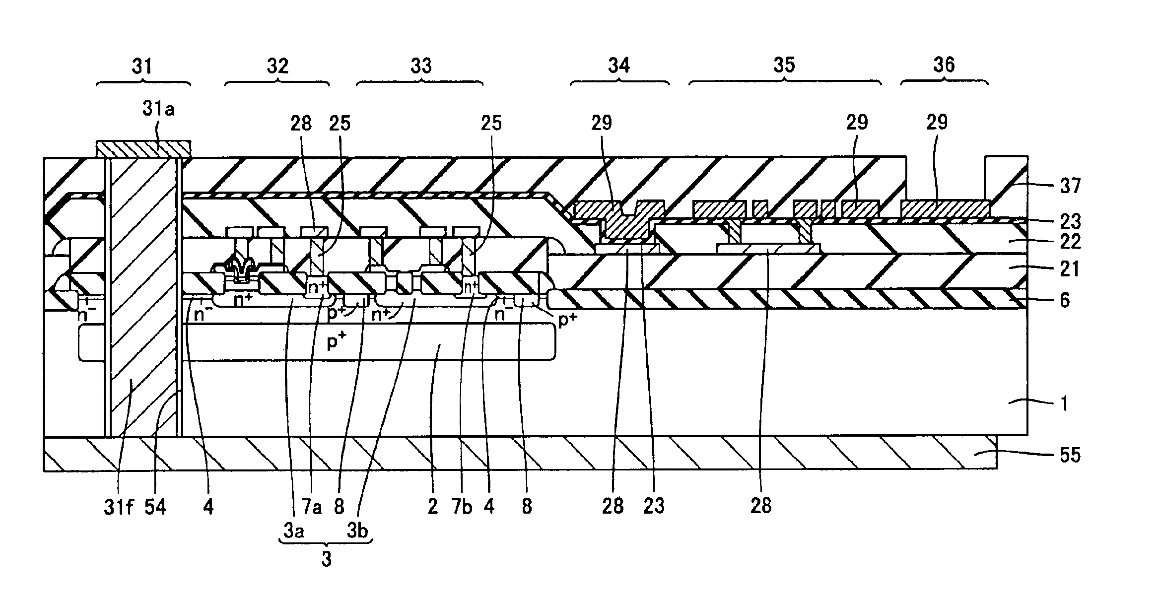
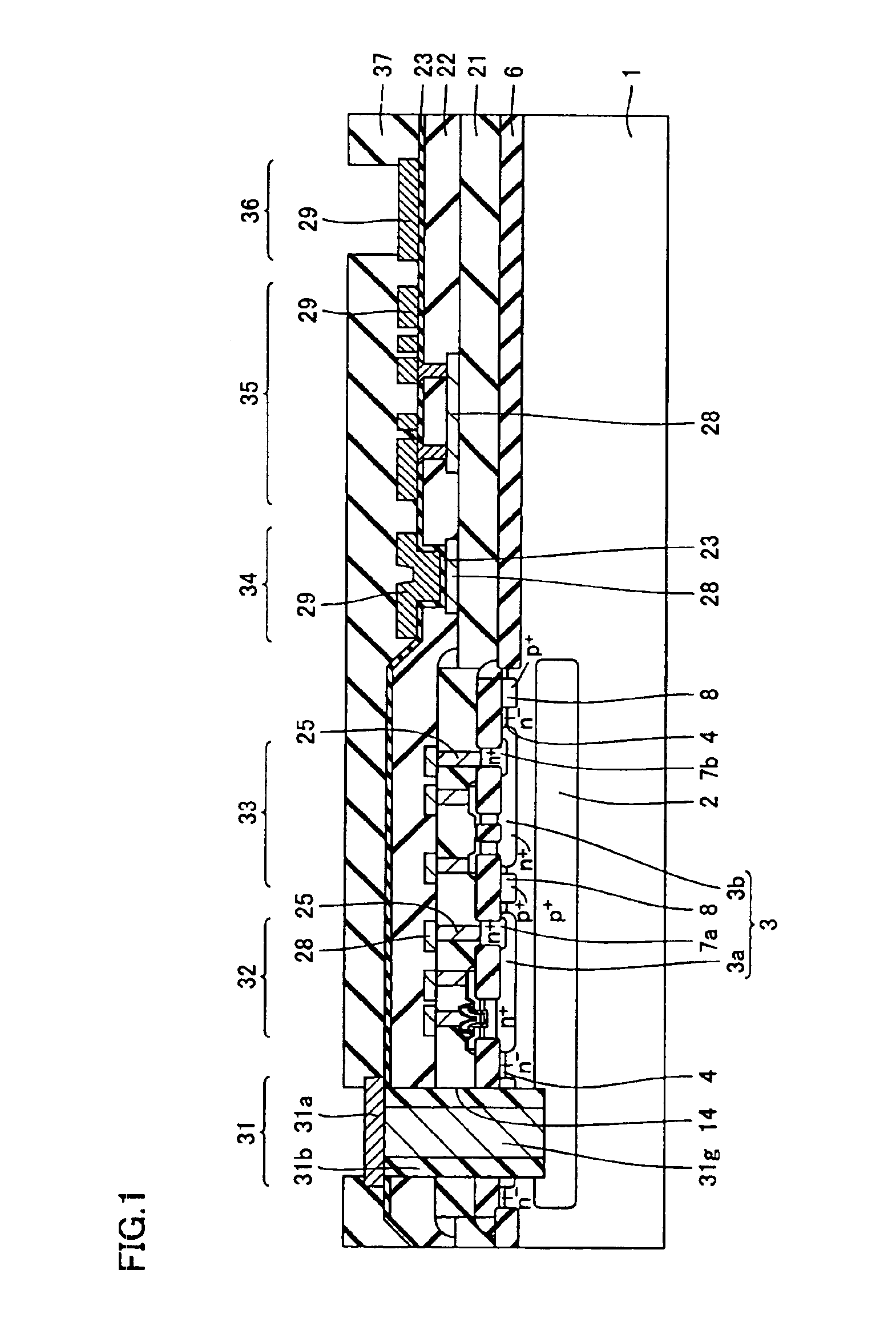
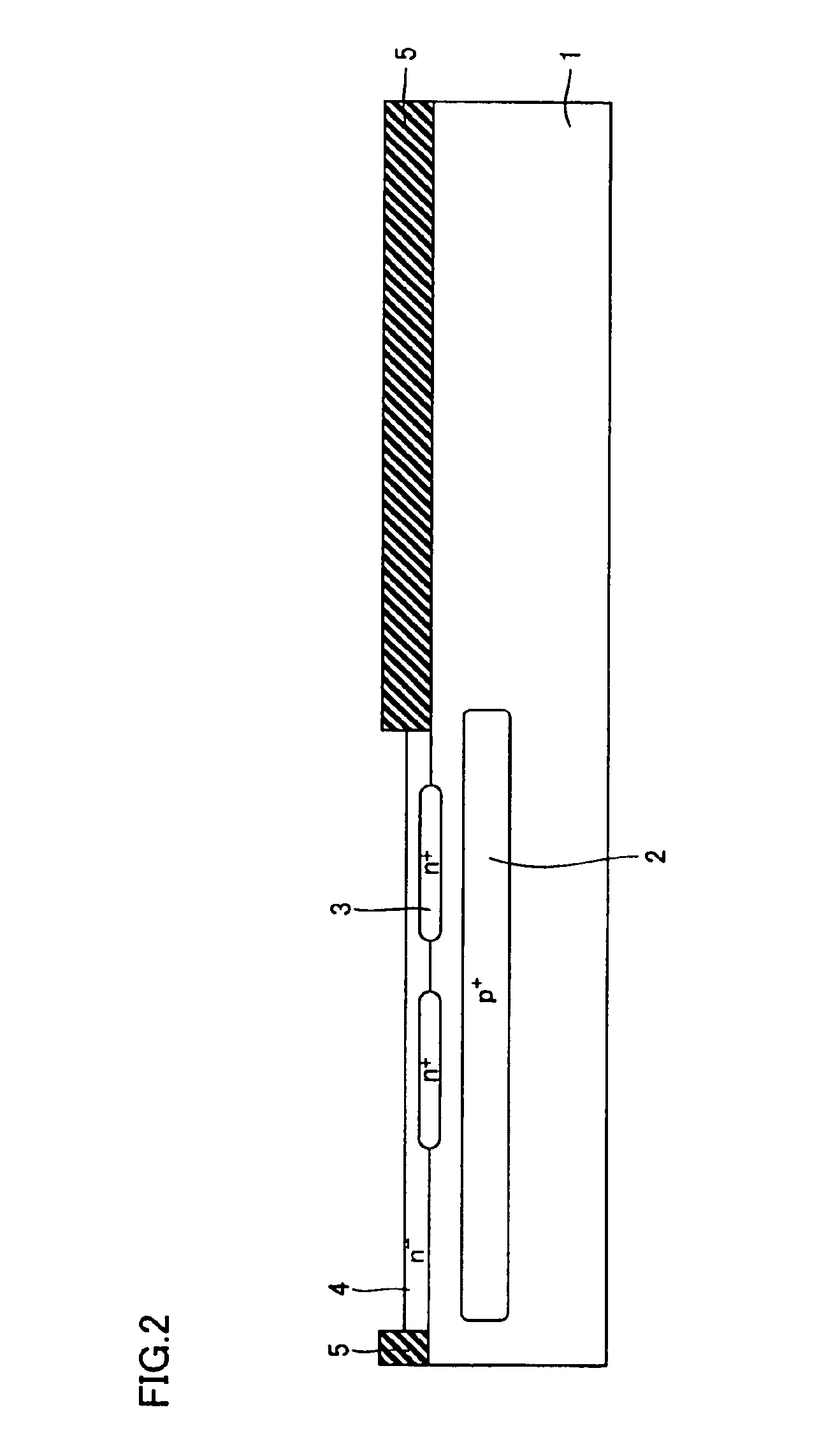
[0037]In FIG. 1, a buried layer 2 of a p conductive type is placed in an Si substrate 1 having a specific resistance of no less than 100 Ωcm and a vertical npn transistor 32 and a horizontal pnp transistor 33, which are active elements, are provided above this buried layer 2 of the p conductive type. A leading electrode 31 is electrically connected to buried layer 2 of the p conductive type and an electrode portion 31a of the leading electrode is placed on a plug wire 31g so as to be exposed from the upper surface of the semiconductor device. Plug wire 31g of this leading electrode is provided in an opening 14 that penetrates interlayer insulating films 21 and 22 and an epitaxial growth layer 3 located there beneath and reaches to buried layer 2 of the p conductive type. The sidewalls of this opening 14 are covered with an oxide film 31b and a Ti film, a TiN film or an Al film forming leading electrode terminal 31a is provided above oxide film 31b.

[0038]A collecto...

second embodiment

(Second Embodiment)

[0062]A base is formed of SiGe in the semiconductor device according to the second embodiment of the present invention. The configuration of this semiconductor device is the same as in the semiconductor device shown in FIG. 1. The semiconductor device according to the present embodiment is characterized by the point that the base is formed of SiGe and it is easier to understand the characteristics of this device by beginning the description from the manufacturing method.

[0063]The manufacturing method of the semiconductor device according to the present embodiment is the same as in the first embodiment up to the step of FIG. 3. Next, as shown in FIG. 8, an Si epitaxial layer 58, an SiGe epitaxial layer 60 and an Si epitaxial layer 62 are made to sequentially grow from below in this order so as to cover the entirety of the wafer. At this time, an Si film or an SiGe film grows as a polycrystal film above an element isolation insulating film 6. Si epitaxial film 58 fo...

third embodiment

(Third Embodiment)

[0071]In reference to FIG. 14, the third embodiment has a structure wherein a contact of a buried layer 2 of a p conductive type or of a substrate 1 is formed of a layer 31c of a p+ conductive type, formed in an Si substrate and in an epitaxial layer 4 of an n− conductive type, a tungsten (W) plug 31d electrically connected to this layer of the p+ conductive type and an Al wire 31e connected to this W plug. The W plug may be separated into a plurality of pieces or may have a layered structure.

[0072]The above described structure is formed as follows. As the next stage after the process of FIG. 2, as shown in FIG. 15, impurities of a p conductive type are implanted into the opening for a leading electrode provided in an element isolation insulating film 6 so that region 31c of the p+ conductive type is formed. This region of the p+ conductive type is formed so as to be electrically connected to buried layer 2 of the p+ conductive type. After this, the process steps o...


PUM


Abstract

A semiconductor device and a method for manufacturing the device using a semiconductor substrate of a high resistance with improved Q value of a passive circuit element. Leakage current due to an impurity fluctuation, in the high resistance semiconductor substrate and noise resistance of an active element in the high resistance semiconductor substrate are improved. The semiconductor device includes a bipolar transistor at a main surface of and in the semiconductor substrate. The bipolar transistor includes a semiconductor layer of a first conductivity type at a bottom portion of the bipolar transistor and the semiconductor device includes a buried layer of a second conductivity type, located in the semiconductor substrate and facing the semiconductor layer of the first conductivity type.

Description

BACKGROUND OF THE INVENTION[0001]1. Field of the Invention[0002]The present invention relates to a semiconductor device and a method for manufacturing the same, and more particularly to a semiconductor device wherein a silicon substrate of a high resistance is used to secure the Q value of passive elements and to restrict leakage current to the substrate so that noise between elements can be reduced, and a method for manufacturing the same.[0003]2. Description of the Background Art[0004]As mobile terminal apparatuses, such as cellular phones, have come into wide use, the manufacture of high frequency devices at a lower cost has become required. Therefore, research has been carried out concerning the replacement of MMICs (Monolithic Microwave Integrated Circuits), wherein the expensive compound semiconductor GaAs is used, with MMICs or Bi-CMOSs (Complementary Metal Oxide Semiconductor) that use silicon (Si) as a base.[0005]Si into which n conductive type or p conductive type impuriti...

Claims


Application Information

Patent Timeline
IPC IPC(8): H01L21/70H01L21/8249H01L27/06H01L21/331H01L29/732H01L29/737
CPCH01L21/8249H01L27/0635H01L27/0652
Inventor FURUKAWA, TAISUKEYONEDA, YOSHIKAZUIKEDA, TATSUHIKO
Owner MITSUBISHI ELECTRIC CORP
Why Eureka
Try Eureka