

Plasma treatment for copper oxide reduction
a technology of copper oxide and treatment method, which is applied in the direction of chemistry apparatus and processes, semiconductor/solid-state device details, coatings, etc., can solve the problems of high copper oxide oxidation risk, difficult to properly prepare the surface within the small features for subsequent processing, and high processing difficulty
- Summary
- Abstract
- Description
- Claims
- Application Information
AI Technical Summary
Benefits of technology
Problems solved by technology
Method used
Image

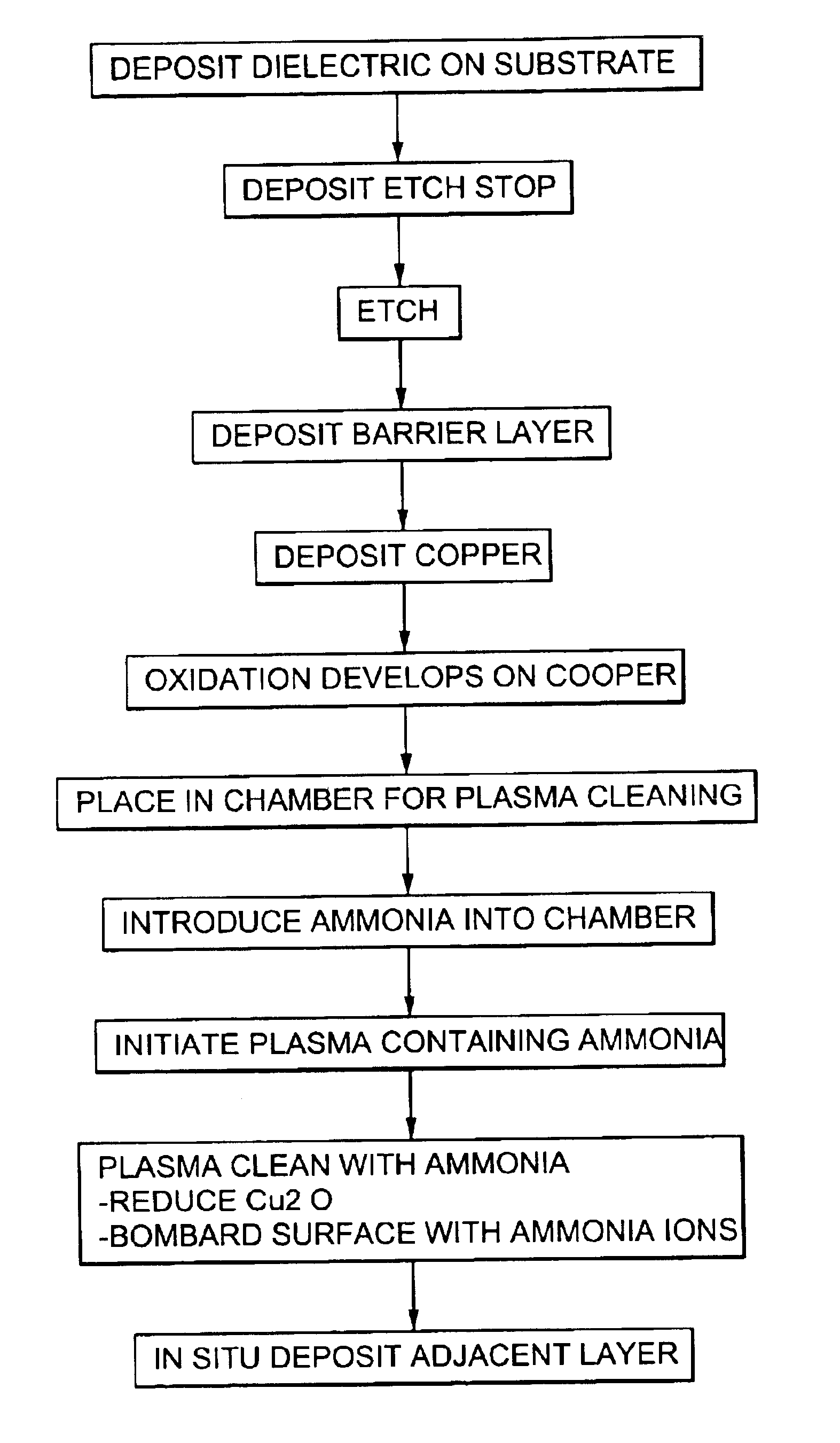
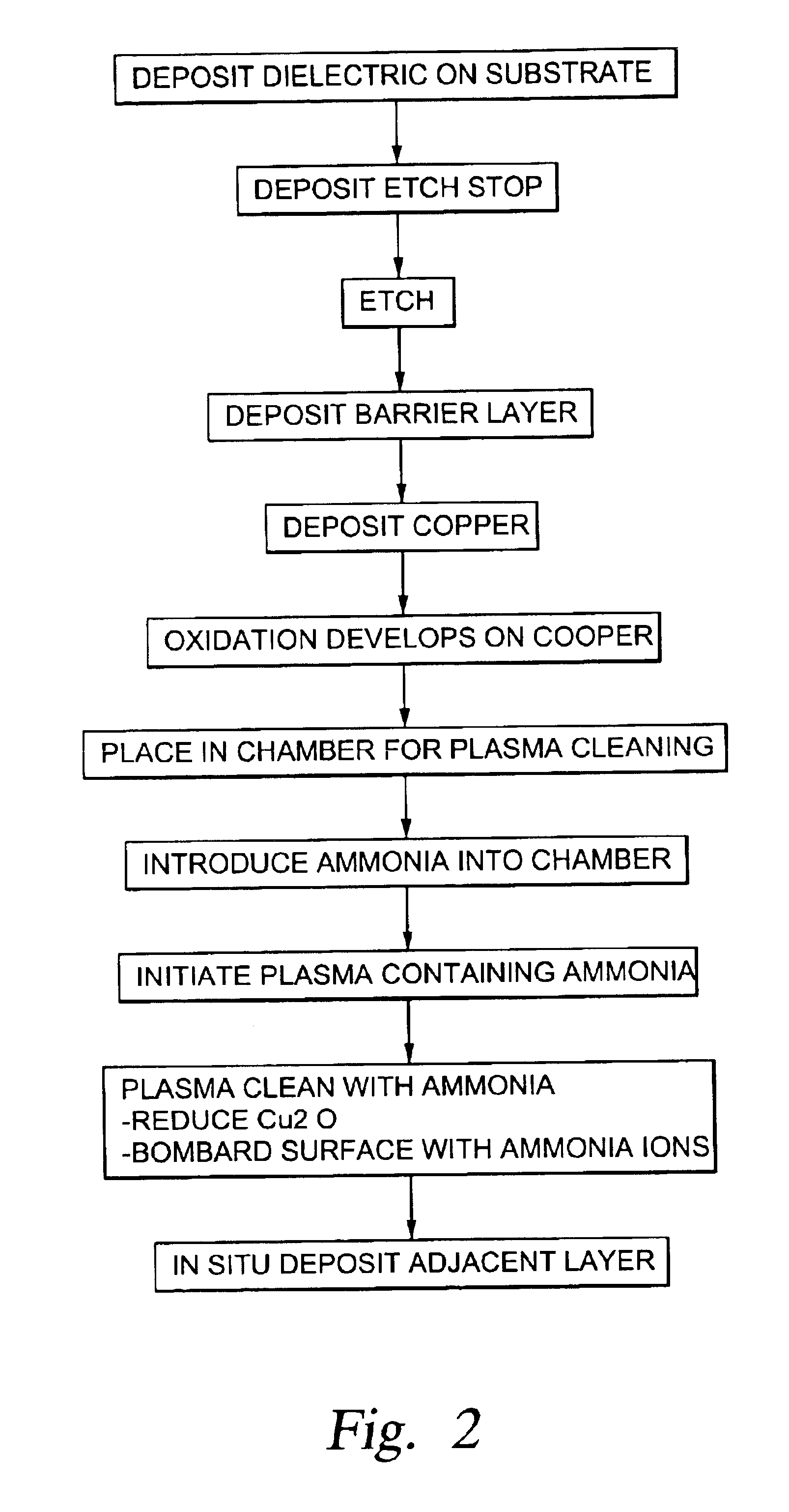
Examples
example 1
Without an Ammonia Plasma Reducing Process
[0033]FIG. 3 shows the oxygen detected through a 500 Å nitride layer deposited on a copper surface after a CMP process without a plasma reducing process. The x-axis represents the binding energy in electron volts (ev), the y-axis represents counts per signal (c / s), and the z-axis represents a relative depth profile through the nitride film layer. The x-axis, showing the binding energy, is element specific and the substrate layers have been tested at an oxygen binding energy level to detect its presence. The y-axis represents the oxygen level detected at an oxygen-specific binding energy. Because the z-axis is relative, the distance between the two largest peaks along the z-axis is the approximate thickness of the 500 Å nitride layer. Beyond the 500 Å nitride layer, the signal count drops to approximately zero because copper is a conductor. FIG. 3 shows a first high peak closest to the origin of the z-axis of ˜11000 c / s. This first and highes...
example 2
With an Ammonia Plasma Reducing Process
[0034]FIG. 4 is a graph corresponding to FIG. 3, showing the results from an exemplary copper surface substrate treated by an ammonia plasma reducing process of the present invention. FIG. 4 can be compared to FIG. 3 and the axes represent similar scales and values. Similar to the substrate surface of FIG. 3, a 500 Å nitride layer was deposited on the copper after applying the plasma reducing process of the present invention. FIG. 4 shows an overall lower oxygen level beyond the initial surface peak, where the initial surface peak may again be ignored for the present purposes. Noticeably, the oxygen level at the nitride / copper interface, represented by the second peak at a depth of about 500 Å, has been lowered to a level of ˜3000 c / s due to the elimination or reduction of the oxide from the copper surface.
[0035]FIG. 5 is a cross-sectional view of a CVD plasma reactor in which the above plasma reducing process may be performed, such as a CENTUR...
PUM
| Property | Measurement | Unit |
|---|---|---|
| temperature | aaaaa | aaaaa |
| surface temperature | aaaaa | aaaaa |
| temperature | aaaaa | aaaaa |
Abstract
Description
Claims
Application Information