Microelectronic components and electronic networks comprising DNA

a technology of electronic networks and microelectronic components, applied in the field of electronic components, can solve the problems of nanoscale circuit construction that cannot be implemented by existing microelectronics technology, the current technology the practicability and theoretical limits of the miniaturization of microelectronics and logics, etc., to achieve the effect of low energy consumption, fast gating, and small siz

Inactive Publication Date: 2005-09-20
TECHNION RES & DEV FOUND LTD
View PDF57 Cites 14 Cited by
  • Summary
  • Abstract
  • Description
  • Claims
  • Application Information

AI Technical Summary

Benefits of technology

[0090]As will obviously be appreciated by the artisan, the formation of the network may be aided by agitating the medium where the network is formed, by providing directional streams of fluid to orient the fibers to connect to a downstream network component at their other end, by applying other biasing measures, etc. In forming wires of the inventions, electric potential between the two ends of the fiber on which the wire is formed, may enhance and provide directional deposition of a conducting substance, e.g. metal.
[0097]While the above network components are useful within the network of the invention, some may at times have utility in different applications. Their small size as compared to corresponding prior art components, allows them to be utilized in a variety of applications requiring a small size or low energy consumption. A particular example of such a component is a wire.

Problems solved by technology

The miniaturization of microelectronics and logics, at current technology, is approaching its practical and theoretical limits.
The construction of nanoscale circuits cannot be implemented by existing microelectronics technology.
In particular, inter element wiring and electrical interfacing to the macroscopic world become increasingly problematic.
However, integrating electronic materials with these structures, or providing them with electronic functionality, has not yet been attained.

Method used


Image

  • Microelectronic components and electronic networks comprising DNA
  • Microelectronic components and electronic networks comprising DNA
  • Microelectronic components and electronic networks comprising DNA

Examples


example 1

Preparation of Linkers

(a) Disulfide Based Linkers:

[0167]Controlled pore glass (CPG) derivatized with a disulfide group is used for the synthesis (starting from its 3′ side) of an oligonucleotide having a free 5′ site. The oligonucleotide is prepared using a conventional DNA synthesizer (see scheme in FIG. 13).

(b) Thiol-Based Linkers:

[0168]Linkers are being prepared according to (a) above and the disulfide bond is cleaved to obtain a free thiol.

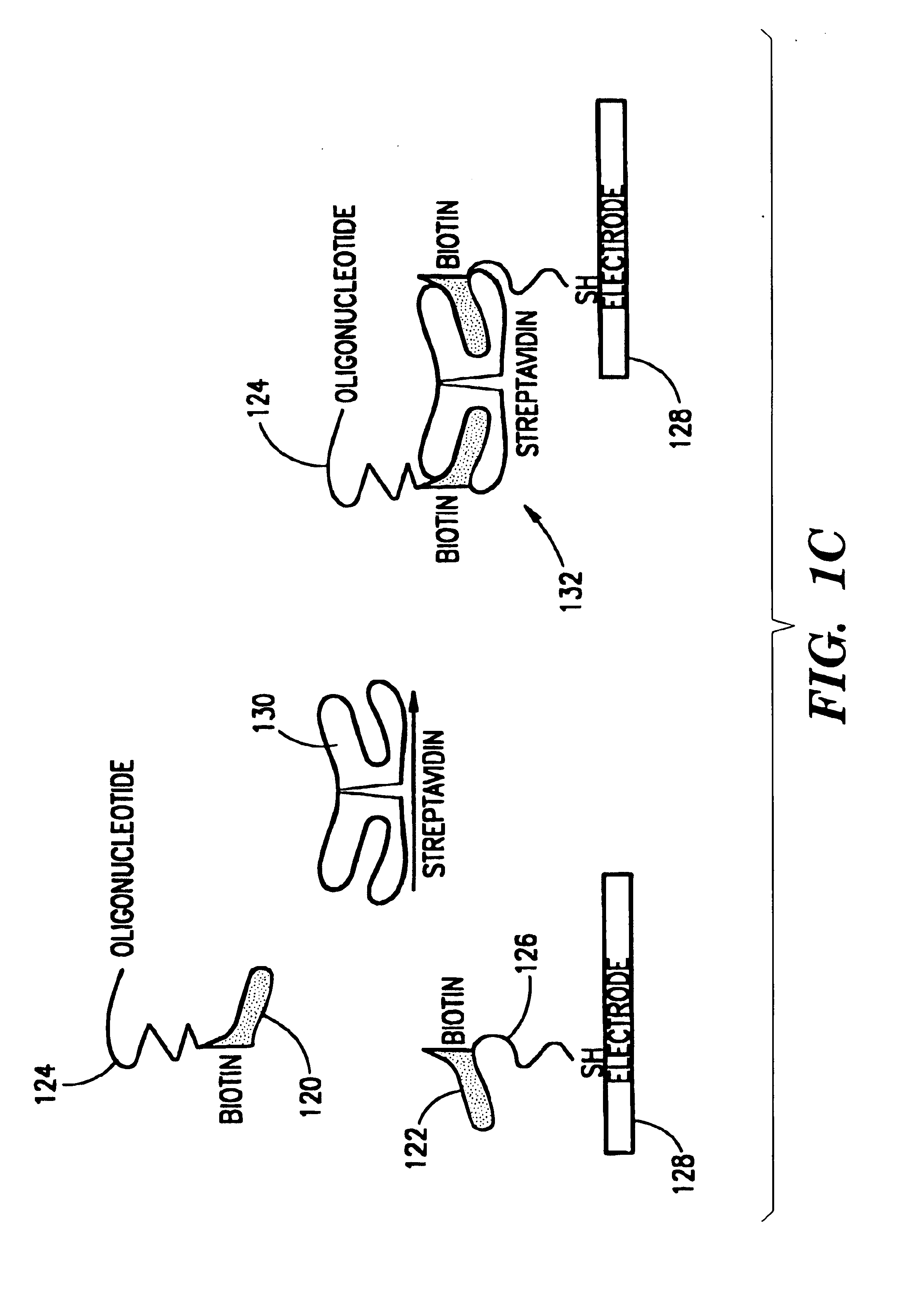
(c) Biotin-Streptavidin Complex Based Linkers:

[0169]Biotin moiety is attached to an oligonucleotide having a specific sequence, as known per se. The biotin-oligonucleotide is coupled via a streptavidin molecule to another molecule containing a biotin moiety at one side (see also FIG. 1C) and a thiol or disulfide group on the other side.

(d) Repressor Based Linkers:

[0170]A nucleic acid binding protein, such as the lac repressor, is covalently attached to a thiol group. A DNA sequence is synthesized having sticky ends and containing the target se...

example 2

Attachment of the Linker to an Electrode

(a) Micropipette Wetting:

[0173]Electrodes are exposed to solutions of the appropriate linkers, for example, by employing pipettes or micropipettes or by any liquid dispensers. Such liquid dispensers may be fixed onto a manipulator that may be computer controlled. Different types of linkers can be deposited on each electrode. Additionally, different types of linkers can be deposited simultaneously or sequentially on different electrodes.

(b) Jet Printing:

[0174]Ink-jet like printing techniques are used for the selective exposure of different electrodes to different linkers. By utilizing such a technique, it is possible to attain high precision, resolution and to increase rates of production, facilitating large scale production.

(c) Ab-Initio Electrode-Linker Synthesis:

[0175](c1) Using Selective Masking Techniques:

[0176]The well developed technology used for synthesizing DNA sequences may be harnessed for the ab-initio preparation of a complex elec...

example 3

Construction of Networks—Production of Junctions

(a) Production of a Branched Sequence:

[0184]A stable four-arm branched DNA junction is constructed using for example the following sequences:

[0185]

               C-G               G-C               C-G               A-T               A-T               T-A               C-G               C-GG C A C G A G T   T G A T A C C GC G T G C T C A   A C T A T G G C               C-G               C-G               G-C               A-T               A-T               T-A               G-C               C-G

[0186]Careful planning of the sequences allows the fabrication of complex junctions according to a desired design. This branch sequence may be attached to double-stranded fibers using methods known per se.

(b) Creating a Branch by Enzymatic Reactions:

[0187]The protein recA from E. coli bacteria catalyzes the recombination and construction of a base-paired hybrid to joining two DNA molecules. It can join, in a specific way, a single-stranded DNA ...


PUM

PropertyMeasurementUnit
field sizeaaaaaaaaaa

Abstract

A microelectronic network is fabricated on a fibrous skeleton by binding or complexing electronically functional substances to the nucleic acid skeleton. The skeleton comprises fibers with nucleotide chains. The assembly of the fibers into a network is based on interactions of nucleotide chain portions of different fibers.

Description

FIELD OF THE INVENTION[0001]The present invention is generally in the field of electronics and relates to electronic networks and circuits as well as to components and junctions of such networks or circuits.PRIOR ART[0002]Prior art believed to be relevant as background of the invention as well as to manufacture or experimental techniques described herein is listed below:[0003]1. Averin, D. V. and Likharev, K. K., in Mesoscopic Phenomena in Solids, eds. Altshuler B., Lee P., and Webb, R., Elsevier, Amsterdam, p. 173, 1991.[0004]2. Grabert H., and Devoret M., eds., Single Charge Tunneling, Plenum, New York, 1992.[0005]3. Kastner, M. A., Rev. Mod. Phys. 64:849, 1992.[0006]4. Porath, D. and Milloh, O., J. Appl. Phys., 85:2241, 1997.[0007]5. Meirav, U. and Foxman, E. B., Semiconductor Science and Technology, 11:255, 1996.[0008]6. Kouwenhoven, L. P. et al., Proceedings of the Advanced Study Institute on Mesoscopic Electron Transport. Kouwenhoven, L. P., Schon, G., and Sohn, L. L. eds., Kl...

Claims


Application Information

Patent Timeline
Patent Type & Authority Patents(United States)
IPC IPC(8): G06N3/12G06N3/00G11C13/02H01L51/30H01L51/05H01L49/00C12Q1/68G06F15/80H01L21/00H01L29/66H01L51/00H01L51/10H01L51/40
CPCB82Y10/00G06N3/123G11C13/0014G11C13/0019H01L51/0093H01L51/0595H01L51/0036H01L51/0038H01L51/0062H10K85/114H10K85/113H10K85/649H10K85/761H10K10/701H10K71/10
Inventor BRAUN, EREZEICHEN, YOAVSIVAN, URIBEN-JOSEPH, GDALYAHU
Owner TECHNION RES & DEV FOUND LTD
Why Eureka
Try Eureka