
Method for integrated in-situ cleaning and subsequent atomic layer deposition within a single processing chamber

a processing chamber and in-situ cleaning technology, applied in chemical vapor deposition coatings, coatings, electric discharge tubes, etc., can solve the problems of poor electrical connection, oxidation of exposed underlying metals, and high via or contact resistance, so as to enhance the overall stack performance

Inactive Publication Date: 2005-09-27
NOVELLUS SYSTEMS
View PDF13 Cites 38 Cited by
  • Summary
  • Abstract
  • Description
  • Claims
  • Application Information

AI Technical Summary

Benefits of technology

The present invention is about a method and apparatus for cleaning and treating high aspect ratio features on substrates before depositing thin films. The method uses halogen or hydrogen containing radicals and argon ions to remove surface contaminants without redepositing them or damaging the feature profile. The cleaning and surface treatment can be performed in-situ without air breaks or substrate transfer under vacuum. The method can be used with different precursors to create various films with different compositions and properties. The cleaning and surface treatment can be controlled by adjusting the precursor flux, halogen or hydrogen containing radical flux, ion flux, or ion energy. The method is compatible with low-k materials and can be performed at low substrate temperatures.

Problems solved by technology

In addition, oxidation of the exposed underlying metal occurs due to exposure to atmosphere or to any oxygen-containing environment.
These oxides (e.g., oxides of Al, Cu, or Si) and residue (e.g., carbonaceous residue from the resist mask used during the etching process) cause poor electrical connection (i.e., high via or contact resistance) and poor reliability (e.g., early electromigration failure).
This makes wet etching inadequate and unattractive due to its inability to clean the bottoms of deep narrow vias and the possibility of contamination from particulates in the cleaning solution.
However, when aspect ratios are high (e.g., greater than 4:1), unwanted material sputtered from the bottoms of vias can redeposit onto the via sidewalls.
This effect will lead to poor mechanical adhesion between subsequently deposited metal film(s) and the contaminated dielectric via sidewalls.
In copper metallization, these redeposited sidewall contaminants can lead to sidewall voiding during the copper electroplating fill process, thus reducing the effective via cross-sectional area.
In addition, sidewall contaminants that are not removed are incorporated as undesirable material inclusions, poisoning the via fill-metal.
Both of these effects serve to increase the overall via resistance, degrade device performance, and reduce interconnect reliability.
A further drawback with argon physical sputtering is that the shapes of patterned features can be altered which may impact device design rules.
If such exposure does occur, then the undesired native oxide and / or contamination will again form on the freshly cleaned substrate interfaces thus defeating the purpose of the preceding step as a preparation for subsequent deposition.
Separate cleaning chambers can have materials present in the background ambient environment, even at reduced pressures, which can adversely influence interfacial properties (e.g., adhesion to and / or crystal orientation of the subsequent film(s) to be deposited) of both the patterned dielectric and the exposed underlying conductor.
In addition, low-k dielectric films exhibit weaker adhesion properties than traditional silicon dioxide.
As an example, fluorine-doped SiO2 (FSG) suffers from poor adhesion properties due to weakly bonded interfacial fluorine (F).
Fluorine attack will compromise the effectiveness of the diffusion layer, leading to poor barrier performance, high via resistance, Cu void formation during electroplating, and delamination (peeling) during chemical mechanical planarization (CMP).

Method used


Image

  • Method for integrated in-situ cleaning and subsequent atomic layer deposition within a single processing chamber
  • Method for integrated in-situ cleaning and subsequent atomic layer deposition within a single processing chamber
  • Method for integrated in-situ cleaning and subsequent atomic layer deposition within a single processing chamber

Examples


Embodiment Construction

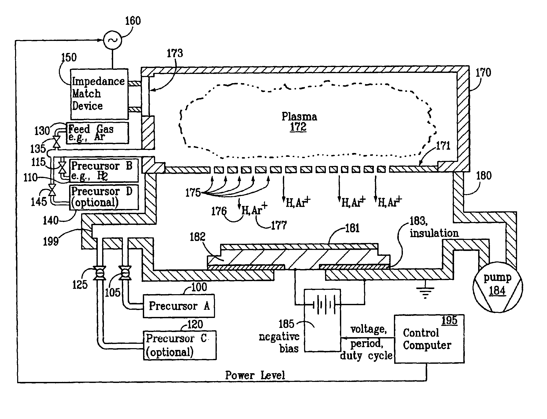
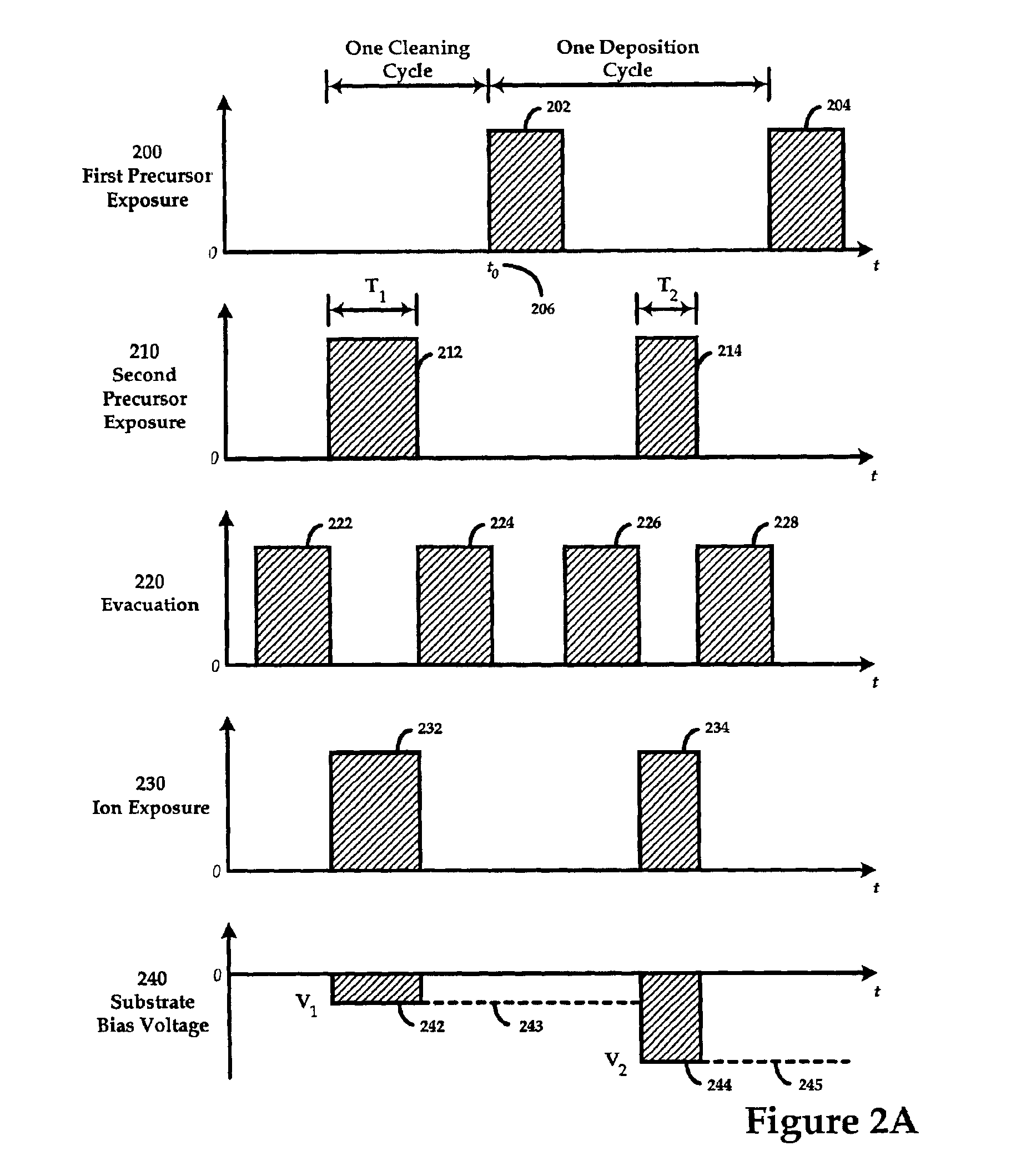
[0023]FIG. 1 illustrates an apparatus suitable for in-situ preclean / surface treatment followed by MII-ALD deposition. A description of the MII-ALD process and apparatus is described in the MII-ALD application and will not be repeated in detail here for brevity. Although the MII-ALD process can be sequential or continuous in nature, both processes involve the reaction of a first and second precursor subject to ion exposure such that the ions deliver the necessary activation energy required for deposition to the near surface atoms and adsorbed reactant(s) via collision cascades.

[0024]As discussed previously, the quality of a deposited film is significantly affected by the cleanliness of the substrate surface prior to deposition. Therefore, in practice, the MII-ALD process should be preceded by a surface cleaning step, most preferably in-situ. The MII-ALD process and associated apparatus, invoked in the absence of a first precursor, is an effective in-situ cleaning process and will be ...


PUM

PropertyMeasurementUnit
temperaturesaaaaaaaaaa
frequenciesaaaaaaaaaa

Abstract

A system and sequential method for integrated, in-situ modification of a substrate and subsequent atomic layer deposition of a thin film onto the substrate in an evacuated chamber includes introducing at least one feed gas into the chamber; generating a plasma from the feed gas; exposing said substrate to ions and / or radicals formed by the plasma; modulating any ions; reacting the substrate with said modulated ions and / or radicals to remove any contaminants from the substrate and producing a modified substrate. These steps are followed, in-situ, by performing an atomic layer deposition of a thin film onto the modified substrate in the chamber including introducing a first reactant gas into said chamber; adsorbing at least one monolayer of the first reactant gas onto the modified substrate; evacuating any excess first reactant gas from the chamber; introducing at least one additional feed gas into the chamber, generating a second plasma from the additional feed gas; exposing the modified substrate to additional ions and / or radicals formed by the plasma; modulating any additional ions; and reacting the adsorbed monolayer of the first reactant gas with any modulated additional ions and / or radicals to deposit the thin film.

Description

CROSS-REFERENCE TO RELATED APPLICATIONS[0001]This application claims the benefit of U.S. Provisional Application No. 60 / 254,280, filed Dec. 6, 2000, U.S. Provisional Application No. 60 / 255,812, filed Dec. 15, 2000, and U.S. application Ser. No. 09 / 812,352, filed Mar. 19, 2001.BACKGROUND OF THE INVENTION[0002]The present invention relates generally to the field of advanced thin film deposition methods commonly used in the semiconductor, data storage, flat panel display, as well as allied or other industries. More particularly, the present invention relates to an in-situ preclean apparatus and technique suitable for cleaning and treatment of high aspect ratio features prior to the deposition of conductive, semi-conductive, and non-conductive thin films via modulated ion-induced atomic layer deposition (MII-ALD).BRIEF DESCRIPTION OF THE PRIOR ART[0003]Semiconductor integrated circuit (IC) manufacturing is a layer-by-layer process utilizing a series of deposition and etching steps. Line...

Claims


Application Information

Patent Timeline
Patent Type & Authority Patents(United States)
IPC IPC(8): C23C16/44C23C16/02C23C16/46C23C16/48C23C16/50C23C16/515C23C16/455H01J37/32H01L21/285H01L21/02H01L21/70H01L21/768C23C16/06C23C16/08C23C16/34C23C16/40
CPCC23C16/0227C23C16/4412C23C16/455C23C16/45525C23C16/45536C23C16/45542C23C16/45544C23C16/45557C23C16/46C23C16/466C23C16/481C23C16/515H01J37/3244H01J37/32449H01J37/32862H01L21/28562H01L21/76814H01L21/76838Y10S438/935
Inventor CHIANG, TONY P.LEESER, KARL F.
Owner NOVELLUS SYSTEMS
Learn More