Planar polymer memory device

a polymer memory and polymer technology, applied in thermoelectric devices, instruments, nanoinformatics, etc., can solve the problems of increasing the volume, use and complexity of computers and electronic devices, reducing the storage density of data, so as to facilitate the construction of high-density memory devices, short resistance/impedance switch time, and improved density and packing

Inactive Publication Date: 2005-12-20
MONTEREY RES LLC
View PDF18 Cites 51 Cited by
  • Summary
  • Abstract
  • Description
  • Claims
  • Application Information

AI Technical Summary

Benefits of technology

[0013]Another aspect of the present invention relates to systems and methods for fabricating multi-layer organic semiconductor memory devices. Multi-level organic memory structures are provided that can store information within organic material associated with the structures. Such memory structures include a plurality of electrodes, the organic material and a passive layer associated with one of the electrodes. The organic memory structures can be formed in a vertical arrangement, wherein two or more organic memory devices are variously positioned relative to an electrode. In addition, a plurality of vertically arranged stacks can be formed in parallel thus facilitating construction of high-density memory ...

Problems solved by technology

The volume, use and complexity of computers and electronic devices are continually increasing.
However, silicon-based devices are approaching their fundamental physical size limits.
Inorganic solid-state devices are generally encumbered with a complex architecture which leads to high cost and a loss of data storage density.
The volatile semiconductor memories based on inorganic semiconductor material must constantly be supplied with electric current with a resulting heating and high electric power consumption in order to maintain stored information.
Non-volatile semiconductor devices have a reduced data rate and relatively high power consumption and large degree of complexity.
Moreover, as the size of inorganic solid-state devices decreases and integration increases, sensitivity to alignment tolerances increases making fabrication markedly more difficult.
Scaling inorganic solid-state devices raises issues with dopant diffusion lengths.
As dimensions are reduced, the dopant diffusion lengths in silicon are posing difficulties in process design.
However, it is not clear that such accommoda...

Method used


Image

  • Planar polymer memory device
  • Planar polymer memory device
  • Planar polymer memory device

Examples


Embodiment Construction

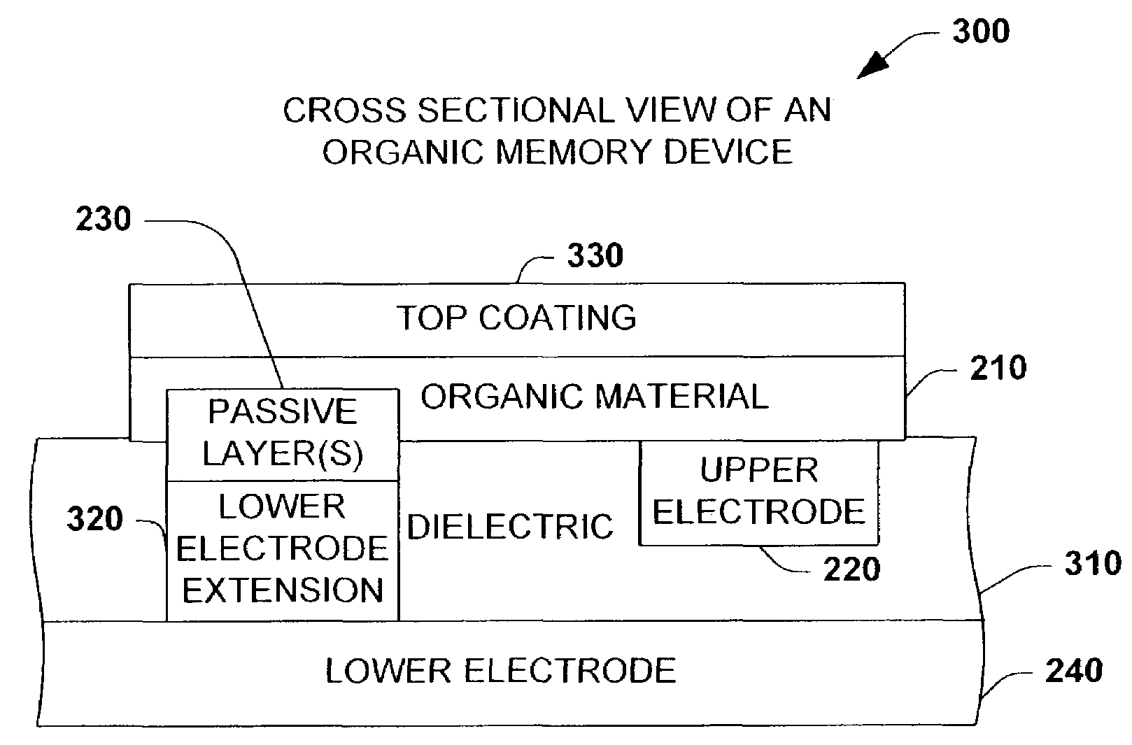
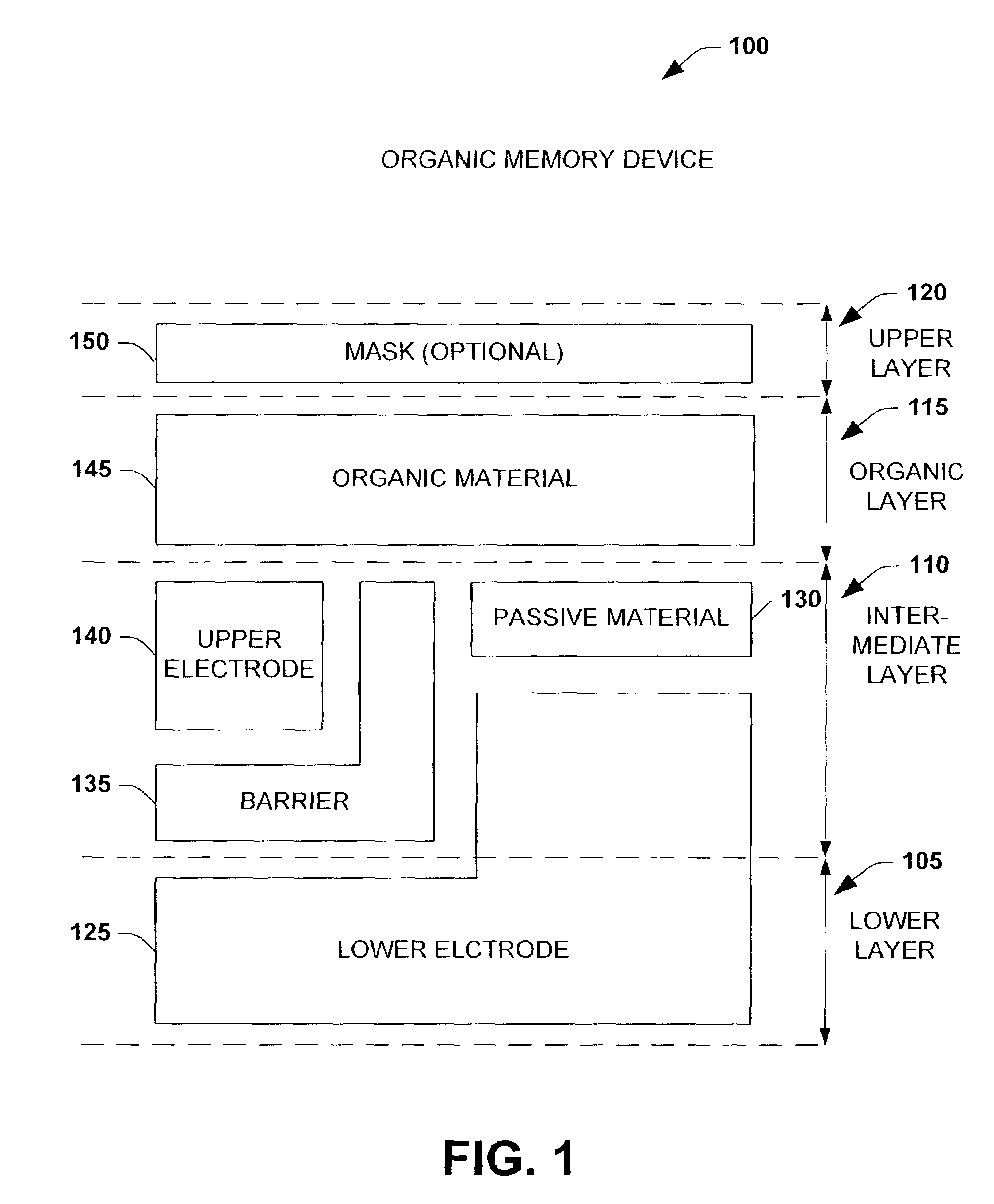
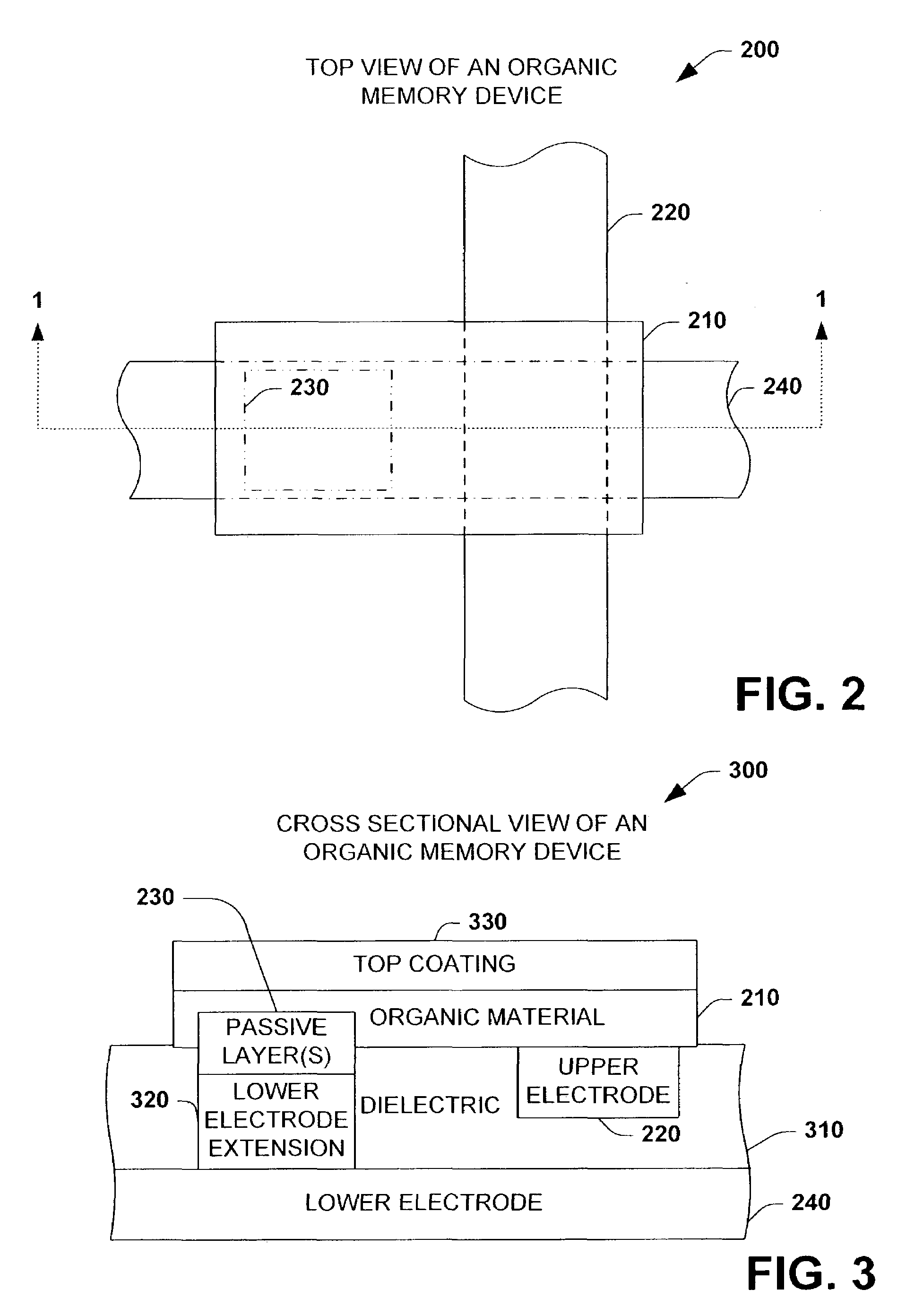
[0034]The present invention provides a planar polymer memory device that can operate as a non-volatile memory device. A single cell memory component can be constructed with two or more electrodes, an electrode extension associated with at least one electrode, a passive layer, a selectively conductive medium operatively coupled to form an individual memory cell, and optionally a partitioning layer to facilitate programming and / or isolate memory cell layers.

[0035]By applying various bias voltages across the two or more electrodes, an impedance state for the memory cell can be stored within the selectively conductive medium. The impedance state can be read by applying a current, and then measuring the impedance state of the selectively conductive medium. The impedance state of the selectively conductive medium represents one or more bits of information, and does not require a persistent power supply or refresh power cycles to retain or maintain a stored impedance state.

[0036]The method...


PUM


Abstract

The present invention provides a planar polymer memory device that can operate as a non-volatile memory device. A planar polymer memory device can be formed with two or more electrodes and an electrode extension associated with one electrode, wherein a selectively conductive medium and dielectric separate the electrodes. The method for forming a planar polymer memory device comprises at least one of forming a first electrode with an associated plug, forming a second electrode, forming a passive layer over the extension, depositing an organic polymer and patterning the organic polymer. The method affords integration of a planar polymer memory device into a semiconductor fabrication process. A thin film diode (TFD) can further be employed with a planar polymer memory device to facilitate programming. The TFD can be formed between the first electrode and the selectively conductive medium or the second electrode and the selectively conductive medium.

Description

FIELD OF INVENTION[0001]The present invention relates generally to organic memory devices and, in particular, to planar polymer memory devices.BACKGROUND OF THE INVENTION[0002]The volume, use and complexity of computers and electronic devices are continually increasing. Computers consistently become more powerful, new and improved electronic devices are continually developed (e.g., digital audio players, video players). Additionally, the growth and use of digital media (e.g., digital audio, video, images, and the like) have further pushed development of these devices. Such growth and development has vastly increased the amount of information desired / required to be stored and maintained for computer and electronic devices.[0003]Memory devices generally include arrays of memory cells. Each memory cell can be accessed or “read”, “written”, and “erased” with information. The memory cells maintain information in an “off” or an “on” state (e.g., are limited to 2 states), also referred to ...

Claims


Application Information

Patent Timeline
IPC IPC(8): G11C11/56G11C13/02H01L27/115H01L27/24H01L27/28
CPCB82Y10/00G11C11/5664G11C13/0014G11C13/0016H01L51/0575H01L27/28H10K19/00H10K10/20
Inventor TRIPSAS, NICHOLAS H.BUYNOSKI, MATTHEW S.OKOROANYANWU, UZODINMAPANGRLE, SUZETTE K.
Owner MONTEREY RES LLC
Why Eureka
Try Eureka