Ceramic and method of manufacturing the same, dielectric capacitor, semiconductor device, and element

a technology of ceramic and manufacturing method, which is applied in the direction of solid-state device, metallic material coating process, chemical vapor deposition coating, etc., can solve the problem of complex manufacturing process of ferroelectric memory

Inactive Publication Date: 2006-03-07
SEIKO EPSON CORP
View PDF20 Cites 14 Cited by
  • Summary
  • Abstract
  • Description
  • Claims
  • Application Information

AI Technical Summary

Benefits of technology

[0009]A method of manufacturing a ceramic according to another aspect of the present invention comprises forming a film which includes a complex oxide material having an oxygen octahedral structure and a paraelectric material having a catalytic effect for the complex oxide material in a mixed state, and performing a heat treatment to the film, wherein the paraelectric material is one of a layered catalytic substance which includes Si in the constituent elements

Problems solved by technology

This gives rise to problems such as complexity of th

Method used


Image

  • Ceramic and method of manufacturing the same, dielectric capacitor, semiconductor device, and element
  • Ceramic and method of manufacturing the same, dielectric capacitor, semiconductor device, and element
  • Ceramic and method of manufacturing the same, dielectric capacitor, semiconductor device, and element

Examples


example 1

[0362]In this example, a Bi4Ti3O12 (BIT) film, a Bi3.3La0.7Si0.7Ti2.25O12 (BLST) film, and a Bi3.3La0.7Si0.35Ge0.35Ti2.25O12 (BLSGT) film formed on a Pt electrode were examined. In this example, a pressure post-annealing step was not performed.

[0363]A sol-gel solution for forming a (Bi, La)4(Si, Ge, Ti)3O12 ferroelectric was prepared by mixing a sol-gel solution for forming BIT and sol-gel solutions for forming La2SiO5 and La2GeO5. La2SiO5 (LSO) and La2GeO5 (LGO) are layered catalytic oxides.

[0364]A sol-gel solution for forming BLST is a solution in which 0.2 mol of LSO was added to 1 mol of the BIT sol-gel solution. A sol-gel solution for forming BLSGT is a solution in which 0.1 mol of LSO and 0.1 mol of LGO were added to 1 mol of the BIT sol-gel solution.

[0365]As a substrate, an Si substrate coated with Pt (Pt / Si substrate) was used. Thin films with a thickness of 100 nm were formed using the sol-gel solutions for forming a ferroelectric prepared by the above procedure by using sp...

example 2

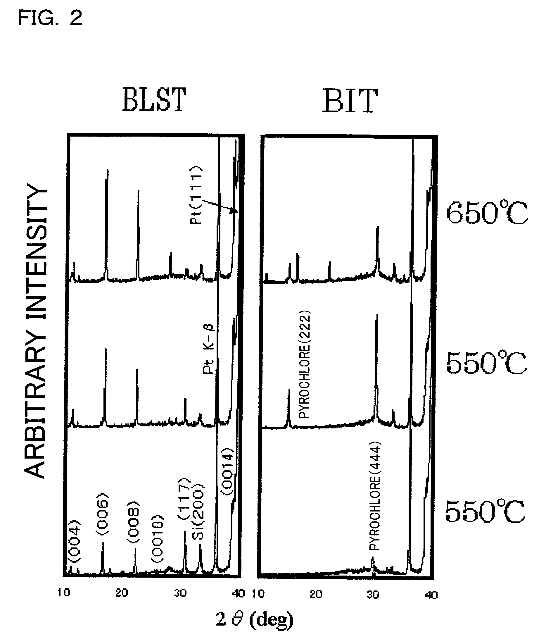
[0377]Each capacitor obtained in Example 1 was subjected to pressure annealing at 500° C. for 30 min. at an oxygen partial pressure of 1 atm. or more. XRD patterns and leakage characteristics of these capacitors were evaluated. FIGS. 4 and 5 show results for the XRD patterns and leakage current density. In the evaluation of the XRD pattern, the pressure of pressure annealing was set at 1.5 atm., 5 atm., and 9.9 atm. In the evaluation of leakage current density, the pressure was set at 1 atm. (without applying pressure), 3 atm., 6 atm., and 9.9 atm.

[0378]As is clear from the XRD patterns shown in FIG. 4, BIT showed a tendency in which the XRD peak became broad by applying a pressure. The XRD peak of BLST shifted to the higher angle side as the pressure was increased, and the XRD peak intensity was increased. The same tendency as BLST was confirmed for BLSGT. Occurrence of a phenomenon in which the XRD peak shifted to the higher angle side and the XRD peak intensity was increased sugg...

example 3

[0386]In this example, changes in properties when changing the amount of Bi2SiO5 (BSO) from 0.1 mol (R=0.1) to 9 mols (R=9) for 1 mol of a ferroelectric material BIT were examined. The film thickness was 100 nm and the crystallization temperature was 600° C. Pressure annealing was performed at 500° C. for three hours in oxygen at 9.9 atm. Capacitors were obtained in the same manner as in Example 1 except for the above conditions. XRD patterns and D–E hysteresis characteristics of the capacitors were evaluated. The results are shown in FIGS. 11 and 12.

[0387]As shown in FIG. 11, the peak of BSO was not observed in the XRD pattern in the range of 0.1≦R≦1. As shown in FIG. 12, good hysteresis characteristics were obtained in the evaluation of the D–E hysteresis characteristics when R=0.1 to 1. The hysteresis shape was improved as the value for R (molar ratio of catalytic oxide to ferroelectric material) was increased.

[0388]As shown in FIG. 11, the peaks of BIT and BSO were observed at t...


PUM

PropertyMeasurementUnit
Pressureaaaaaaaaaa
Molar ratioaaaaaaaaaa
Superconductivityaaaaaaaaaa

Abstract

A method of manufacturing a ceramic includes forming a film which includes a complex oxide material having an oxygen octahedral structure and a paraelectric material having a catalytic effect for the complex oxide material in a mixed state, and performing a heat treatment to the film, wherein the paraelectric material is one of a layered catalytic substance which includes Si in the constituent elements and a layered catalytic substance which includes Si and Ge in the constituent elements. The heat treatment includes sintering and post-annealing. At least the post-annealing is performed in a pressurized atmosphere including at least one of oxygen and ozone. A ceramic is a complex oxide having an oxygen octahedral structure, and has Si and Ge in the oxygen octahedral structure.

Description

BACKGROUND OF THE INVENTION[0001]The present invention relates to a ceramic and a method of manufacturing the same, a dielectric capacitor, a semiconductor device, and other elements including the ceramic of the present invention.[0002]As a ferroelectric film applied to semiconductor devices (ferroelectric memory (FeRAM), for example), a ferroelectric film having a perovskite structure (PbZrTiO-type ferroelectric film, for example) and a ferroelectric film having a layered perovskite structure (BiLaTiO-type, BiTiO-type, or SrBiTaO-type ferroelectric film, for example) have been proposed. The ferroelectric film having a layered perovskite structure is generally formed by crystal growth from an amorphous state.[0003]In the case of forming a ferroelectric film having a layered perovskite structure by using this formation method, the crystal growth rate in the c-axis direction becomes lower than those in the a-axis direction and the b-axis direction due to the crystal structure of the f...

Claims


Application Information

Patent Timeline
IPC IPC(8): B05D5/12C23C14/00C23C16/00C04B35/42C04B35/45C04B35/457C04B35/465C04B35/472C04B35/475C04B35/491C04B35/493C04B35/495C04B35/497C04B35/624C23C14/08C23C16/40C23C18/12H01L21/314H01L21/316H01L21/8246H01L41/22H01L41/314H01L41/317H01L41/318H01L41/39
CPCC04B35/01H01L27/11507C04B35/42C04B35/4521C04B35/457C04B35/465C04B35/472C04B35/475C04B35/491C04B35/493C04B35/495C04B35/497C04B35/624C04B35/6264C04B35/62645C04B35/64C23C14/08C23C16/40C23C16/409C23C18/1208C23C18/1225H01L21/02197H01L21/02282H01L21/31691H01L27/11502C04B35/16C04B2235/3205C04B2235/3208C04B2235/3213C04B2235/3215C04B2235/3224C04B2235/3227C04B2235/3232C04B2235/3244C04B2235/3251C04B2235/3256C04B2235/3258C04B2235/3287C04B2235/3296C04B2235/3298C04B2235/3418C04B2235/3427C04B2235/3436C04B2235/3445C04B2235/3454C04B2235/3463C04B2235/664C04B2235/76C04B2235/80H10N30/8561H10N30/078H10B53/30H10B53/00H01L27/105
Inventor NATORI, EIJIKIJIMA, TAKESHIFURUYAMA, KOICHITASAKI, YUZO
Owner SEIKO EPSON CORP
Why Eureka
Try Eureka