Power module with improved heat dissipation

a power module and heat dissipation technology, applied in the field of power modules, can solve the problems of inability to improve thermal conductivity remarkably, difficult to fill inorganic fillers with high density, and difficult to improve heat dissipation structure of power modules, so as to and improve heat dissipation efficiency.

Inactive Publication Date: 2006-05-02
PANASONIC CORP
View PDF11 Cites 32 Cited by
  • Summary
  • Abstract
  • Description
  • Claims
  • Application Information

AI Technical Summary

Benefits of technology

[0012]To solve the above-mentioned problems, the present invention provides a power module that is excellent in heat dissipation and suitable for miniaturization with higher density, and also the present invention provides a method of manufacturing the power module.

Problems solved by technology

The heat dissipating structure of a power module is a key issue for the purposes.
However, since this substrate is produced by melt-kneading a thermoplastic resin and an inorganic filler and injecting this mixture, the inorganic filler is difficult to fill with high density.
As a result, the thermal conductivity cannot be improved remarkably.
Therefore, in a conventional power module to dissipate heat from a semiconductor chip to a substrate, an improvement in heat dissipation cannot be expected when flip-chip bonding is used.
However, since the conductive resistance of the metal wire is considerably great when compared with ON resistance of the semiconductor element, power loss is increased and so is the calorific value when a semiconductor chip is mounted by wire bonding.

Method used


Image

  • Power module with improved heat dissipation
  • Power module with improved heat dissipation
  • Power module with improved heat dissipation

Examples


first embodiment

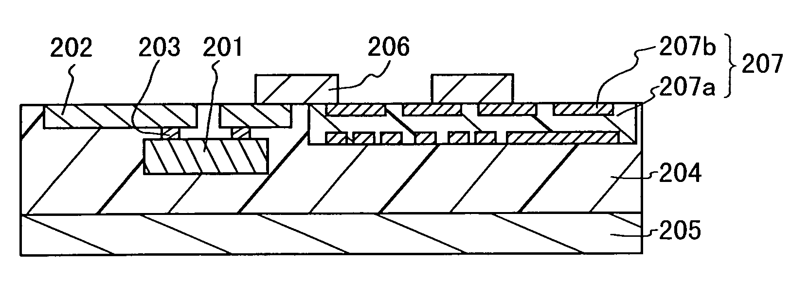
[0123]A power module configured as shown in FIG. 1 was produced in the following process steps. First, a polyphenylene sulphide (PPS) film 50 μm in thickness was prepared as a release carrier and a rubber-based adhesive was applied on the surface of the release carrier to be 10 μm in thickness. A copper foil 250 μm in thickness was bonded to the adhesive-applied surface of the release carrier by a roll-laminate method. After laminating a dry film on the copper foil surface, the dry film was exposed through a mask formed with a wiring pattern, and developed to remove the dry film in a portion other than the exposed portion. Next, unnecessary portions of the copper foil were removed by dipping in a solution of ferric chloride, and then, the dry film was further removed by using sodium hydroxide, so that a lead frame was formed.

[0124]Next, a semiconductor chip was flip-chip mounted on the lead frame. An IGBT for current of 50 A (manufactured by Matsushita Electronics Corporation) was u...

second embodiment

[0134]Sheet-like insulators were produced by printing insulating pastes of the respective compositions shown in Table 1 on PPS films (75 μm in thickness), drying, and further by laminating second PPS films and curing by heat and pressure.

[0135]

TABLE 1ThermosettingColor-Cou-Sam-Inorganic fillersresin compositioningDisper-plingpleAmountAmountagentsantagentNo.Type(wt %)Type(wt %)(wt %)(wt %)(wt %)1Al2O365Epoxy340.50.30.2resin2Al2O390Epoxy90.50.30.2resin3SiO270Epoxy290.50.30.2resin4SiO275Epoxy240.50.30.2resin5SiO280Epoxy190.50.30.2resin6SiO285Epoxy140.50.30.2resin7MgO75Epoxy240.50.30.2resin8MgO85Epoxy140.50.30.2resin9BN75Epoxy240.50.30.2resin10BN85Epoxy140.50.30.2resin

[0136]In this embodiment, an epoxy resin composition compring 90 wt % of bisphenol F epoxy resin (manufactured by Yuka Shell Epoxy Co., Ltd.), 3 wt % of an amine adduct (“MY-H” manufactured by Ajinomoto Co., Inc.) as a hardening agent, and 7 wt % of imidazole as a hardening accelerator was used.

[0137]The Al2O3 was “AS-40” ...

third embodiment

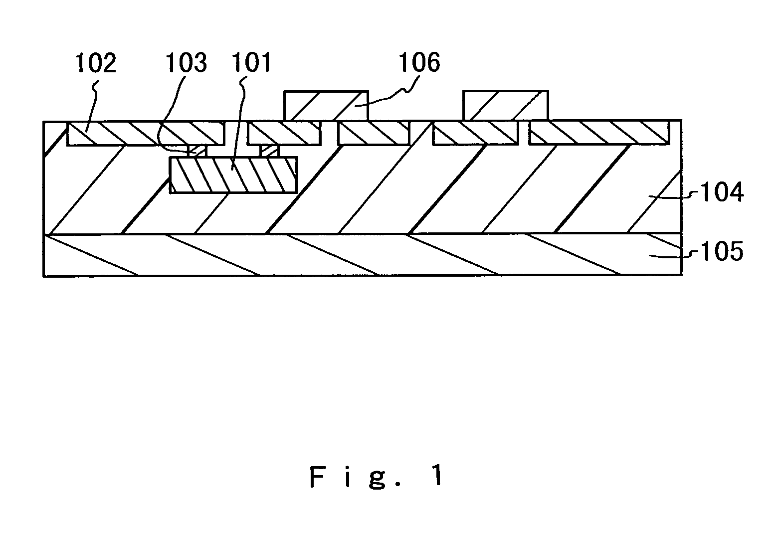
[0146]A power module configured as shown in FIG. 1 was produced in the following manner. First, a lead frame was formed on a release carrier, and a semiconductor chip was flip-chip mounted on the lead frame in the same manner of First Embodiment.

[0147]Next, a solvent of methyl ethyl ketone was added to a resin composition comprising the following substances before rotational mixing in a pot comprising an alumina ball for 48 hours at a speed of 500 rpm to prepare slurry. The amount of the methyl ethyl ketone solvent to be added was controlled to adjust the slurry's viscosity to be about 20 Pa·s.

[0148](1) 85 wt % of AlN (manufactured by Dow Chemical Co. Ltd., the average particle diameter of 12 μm)

[0149](2) 14 wt % of a cyanate resin composition (manufactured by Asahi Ciba with a trade name of “AroCy M-30”)

[0150](3) 0.3 wt % of carbon black (manufactured by Toyo Carbon)

[0151](4) 0.2 wt % of a dispersant (manufactured by Dai-ichi Kogyo Seiyaku Co., Ltd. with a trade name of “Prysurf F-...


PUM


Abstract

The invention provides a power module that is excellent in heat dissipation and suitable for the trend of miniaturization with high density, and provides also a method of manufacturing the same. The power module includes an insulating layer including an inorganic filler and a thermosetting resin composition, a lead formed on the surface of the insulating layer, and a semiconductor chip mounted on a insulating layer side of the lead, and a heat sink formed on the backside of the insulating layer. The semiconductor chip is mounted on the lead by flip-chip bonding and sealed in the insulating layer.

Description

BACKGROUND OF THE INVENTION[0001]1. Field of the Invention[0002]The present invention relates to a power module with a mounted semiconductor chip, and a method of manufacturing the same.[0003]2. Description of the Prior Art[0004]Recently, with a demand for high performance and miniaturization of electronic equipment, smaller power source circuits consuming less power have been increasingly desired in the power electronics field. The heat dissipating structure of a power module is a key issue for the purposes.[0005]In a method proposed to improve heat dissipation of a power module, a substrate with high thermal conductivity is used. A semiconductor chip is mounted on this substrate so that the backside (the side opposite to the device-forming surface) of the semiconductor chip contacts with the surface of the substrate, and heat is dissipated from the substrate.[0006]To achieve this purpose, for example, a method using a metal-base substrate has been proposed. The metal-base substrat...

Claims


Application Information

Patent Timeline
Patent Type & Authority Patents(United States)
IPC IPC(8): H01L23/10H01L23/34
CPCH01L21/568H01L21/6835H01L23/3107H01L23/36H01L23/4951H01L23/4952H01L23/49524H01L23/49575H01L23/5389H01L24/81H01L25/16H01L2924/1305H01L2924/1306H01L2224/16245H01L2224/16H01L2224/81801H01L2924/01013H01L2924/01029H01L2924/01078H01L2924/01079H01L2924/01082H01L2924/01322H01L2924/13055H01L2924/13091H01L2924/3025H01L2924/01006H01L2924/01019H01L2924/01033H01L2924/0105H01L2924/01074H01L2924/014H01L2924/00H01L2924/00011H01L2924/00014H01L2224/0401
Inventor NAKATANI, SEIICHIHIRANO, KOICHIMATSUO, MITSUHIROHANDA, HIROYUKI
Owner PANASONIC CORP
Why Eureka
Try Eureka