High through-put Cu CMP with significantly reduced erosion and dishing

a technology of cu and ccmp, which is applied in the direction of chemistry apparatus and processes, lapping machines, manufacturing tools, etc., can solve the problems of difficult to meet escalating requirements, difficult to achieve a high degree of surface uniformity, and difficult to meet them, so as to reduce erosion, reduce dishing, and eliminate erosion or at least significantly reduce the effect of erosion

Inactive Publication Date: 2006-05-09
APPLIED MATERIALS INC
View PDF40 Cites 14 Cited by
  • Summary
  • Abstract
  • Description
  • Claims
  • Application Information

AI Technical Summary

Benefits of technology

[0013]An advantage of the present invention is a method of planarizing Cu and Cu alloys by CMP at high production through-put with no or significantly reduced erosion and no or significantly reduced dishing.
[0014]Additional advantages and other features of the present invention will be set forth in part in the description which follows and in part will become apparent to those having ordinary skill in the art upon examination of the following or may be learned from the practice of the present invention. The advantages of the present invention may be realized and obtained as particularly pointed out in the appended claims.
[0015]According to the present invention, the foregoing and other advantages are achieved in part by a method of planarizing a wafer surface containing: an interlayer dielectric having an upper surface and a plurality of openings; a barrier layer lining the openings and on the upper surface of the interlayer dielectric; and copper (Cu) or a Cu alloy filling the openings and on the interlayer dielectric; the method comprising the sequential steps of: (a) chemical mechanical polishing (CMP) the wafer to reduce the Cu or Cu alloy layer at a first removal rate to thickness of about 500 Å to about 3,000 Å; and (b) CMP the wafer to remove the Cu or Cu alloy layer at a second removal rate, less than the first removal rate, stopping on the barrier layer.
[0016]Embodiments of the present invention include conducting step (a) at a first removal rate greater than about 5,000 Å per minute and conducting step (b) at a removal rate of about 1000 Å per minute to about 3000 Å per minute. Erosion is eliminated or at least significantly reduced by conducting CMP operations with fixed abrasive polishing pads at a very high selectively of Cu:Ta or Cu: TaN. During CMP, dishing is controlled to no greater than 300 Å as by reducing the platen rotating speed to achieve a polishing pad temperature no greater than about 50° C., thereby reducing the static etching rate and reducing pad deformation, thus reducing dishing. Particles are removed and temperature is reduced during CMP by flowing the chemical agent across the wafer surface at a high flow rate. The chemical agent or mixture can be recycled to reduce the cost of consumables. An inhibitor is flowed across the wafer surface after each CMP step prior to initiating a subsequent step, to reduce the static etching rate.
[0017]Additional advantages of the present invention will become readily apparent to those skilled in this art from the following detailed description, wherein embodiments of the present invention are described, simply by way of illustration of the best mode contemplated for carrying out the present invention. As will be realized, the present invention is capable of other and different embodiments, and its several details are capable of modifications in various obvious respects, all without departing from the present invention. Accordingly, the drawings and description are to be regarded as illustrative in nature, and not as restrictive.

Problems solved by technology

Such escalating requirements have been found difficult to satisfy in terms of providing a low RC (resistance and capacitance) interconnect pattern, particularly wherein submicron vias, contacts and trenches have high aspect ratios imposed by miniaturization.
However, the chemical agent does not contain abrasive particles as in abrasive slurry-type CMP operations.
In applying conventional planarization techniques; such as CMP, to Cu, it is extremely difficult to achieve a high degree surface uniformity, particularly across a surface extending from a dense array of Cu features, e.g., Cu lines, bordered by an open field.
Cu or a Cu alloy is then deposited, as by electroplating, electroless plating, physical vapor deposition (PVD) at a temperature of about 50° C. to about 150° C. or chemical vapor deposition (CVD) at a temperature under about 200° C., typically at a thickness of about 8,000 Å to about 18,000 Å. In planarizing the wafer surface after copper metallization, erosion and dishing are typically encountered, thereby decreasing the degree of surface uniformity or planarity and challenging the depth of focus limitations of conventional photolithographic techniques, particular with respect to achieving submicron dimensions, such as below about 0.25 micron.
Upon removing the barrier layer in the open field, the oxide layer in the dense array is overpolished resulting in erosion.

Method used


Image

  • High through-put Cu CMP with significantly reduced erosion and dishing
  • High through-put Cu CMP with significantly reduced erosion and dishing
  • High through-put Cu CMP with significantly reduced erosion and dishing

Examples


Embodiment Construction

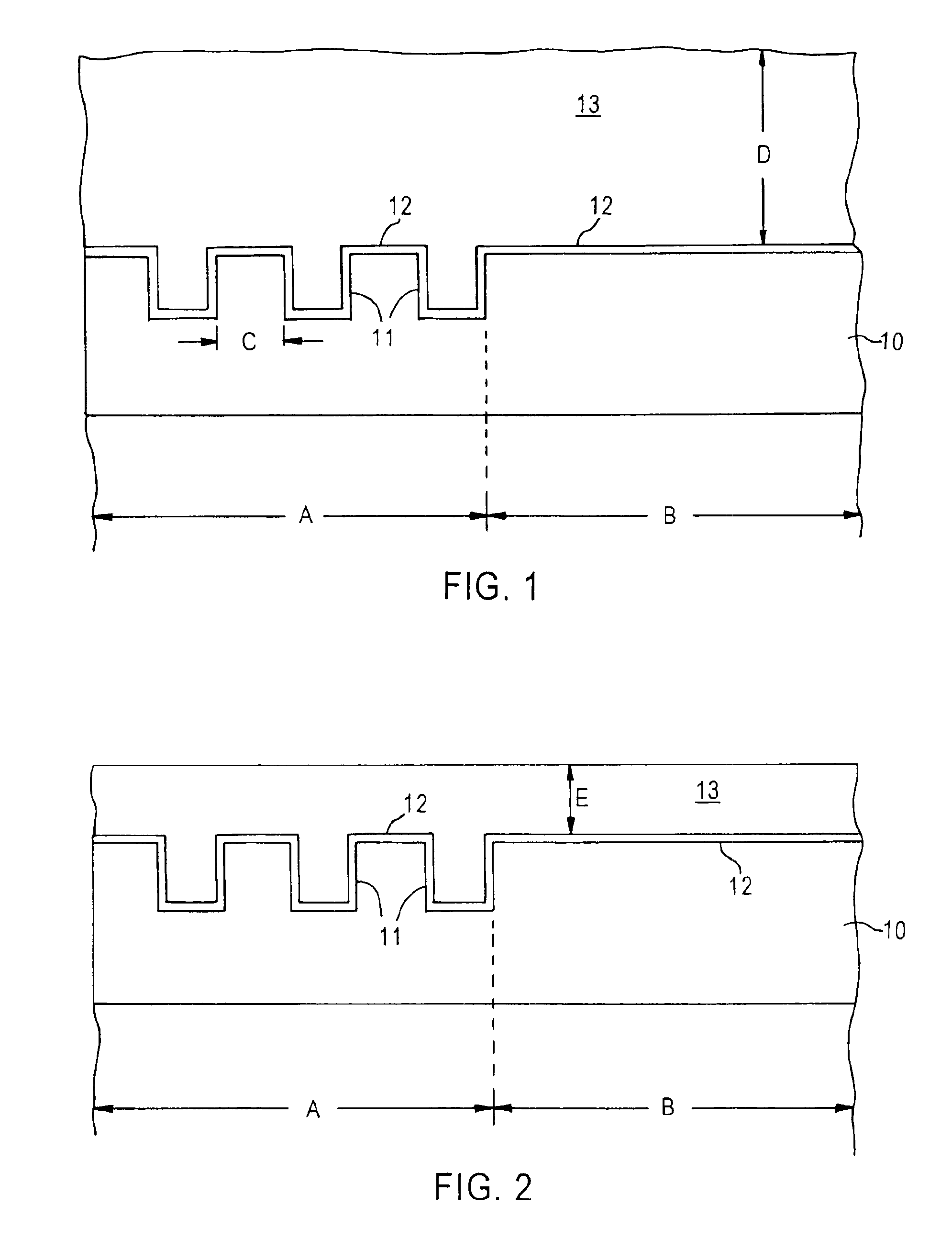
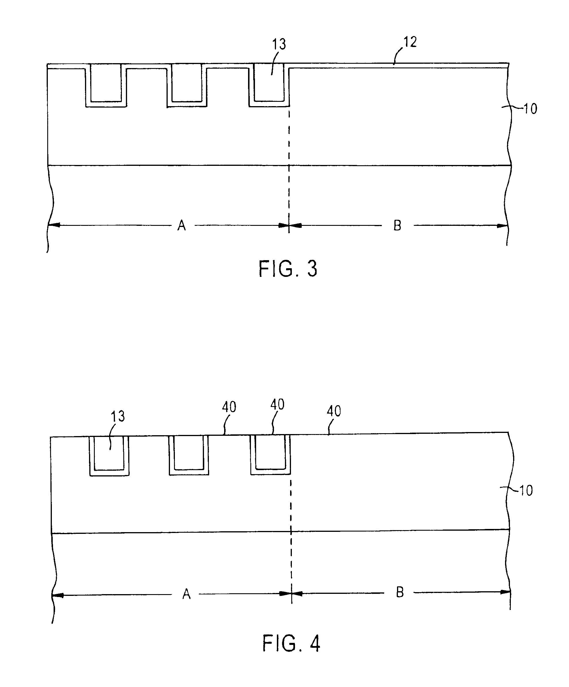
[0020]The present invention achieves the heretofore elusive objective of effectively planarizing Cu metallization at high production through-put while eliminating or substantially reducing both erosion and dishing, consistent with the ever increasing demands for reliable interconnect patterns having feature sizes in the deep submicron range. As used throughout this disclosure, the symbol Cu is intended to encompass high purity elemental copper as well as copper-based alloys, e.g., copper-based alloys containing at least about 80 wt. % copper.

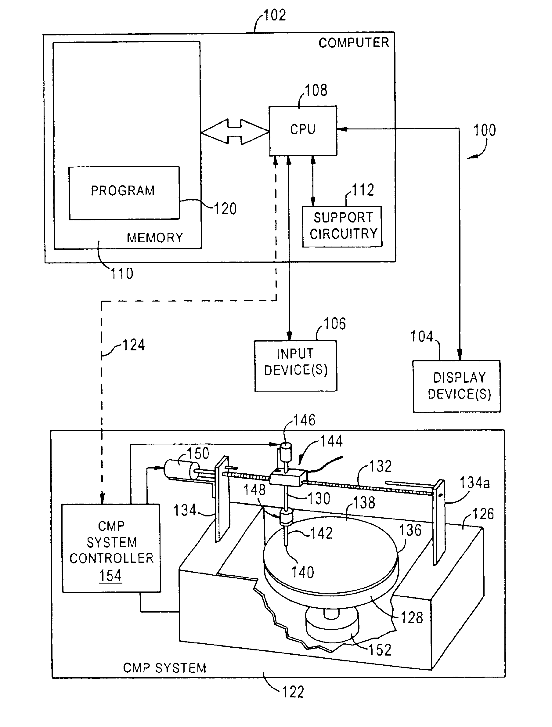
[0021]The objectives of the present invention are achieved by employing a strategic multi-step process comprising sequential CMP steps by fixed abrasive polishing stopping on the barrier layer with no or significantly reduced dishing and erosion, using one or more rotating platens with a polishing pad mounted thereon, or one or more linear belts. Buffing with an abrasive slurry can then be conducted to remove the barrier layer. The multi-step me...


PUM

PropertyMeasurementUnit
wt. %aaaaaaaaaa
pressureaaaaaaaaaa
pressureaaaaaaaaaa

Abstract

High through-put Cu CMP is achieved with reduced erosion and dishing by a multi-step polishing technique. Deposited Cu is polished with fixed abrasive polishing pads initially at a high removal rate and subsequently at a reduced removal rate and high Cu:barrier layer (Ta) selectivity. Embodiments of the present invention include reducing dishing by: controlling platen rotating speeds; increasing the concentration of active chemicals; and cleaning the polishing pads between wafers. Embodiments also include removing particulate material during CMP by increasing the flow rate of the chemical agent or controlling the static etching rate between about 100 Å and about 150 Å per minute, and recycling the chemical agent. Embodiments further include flowing an inhibitor across the wafer surface after each CMP step to reduce the static etching rate.

Description

TECHNICAL FIELD[0001]The present invention relates to copper (Cu) and / or Cu alloy metallization in semiconductor devices with improved planarity. The present invention is applicable to manufacturing high speed integrated circuits having submicron design features and high conductivity interconnect structures with high production throughput.BACKGROUND ART[0002]The escalating requirements for high density and performance associated with ultra large scale integration semiconductor wiring require responsive changes in interconnection technology. Such escalating requirements have been found difficult to satisfy in terms of providing a low RC (resistance and capacitance) interconnect pattern, particularly wherein submicron vias, contacts and trenches have high aspect ratios imposed by miniaturization.[0003]Conventional semiconductor devices comprise a semiconductor substrate, typically doped monocrystalline silicon, and a plurality of sequentially formed dielectric interlayers and conducti...

Claims


Application Information

Patent Timeline
Patent Type & Authority Patents(United States)
IPC IPC(8): H01L21/302B24B37/04B24B57/02H01L21/304H01L21/321
CPCB24B37/04H01L21/3212B24B57/02H01L21/302
Inventor LI, SHIJIANREDEKER, FRED C.WHITE, JOHNEMAMI, RAMIN
Owner APPLIED MATERIALS INC
Why Eureka
Try Eureka