

Low power consumption MIS semiconductor device
a technology of semiconductor devices and low power consumption, applied in the direction of power consumption reduction, pulse technique, instruments, etc., can solve the problems of disadvantageous standby current increase, off-leak current increase, and the threshold voltage cannot be reduced in absolute value, so as to reduce the current dissipation and simple circuit configuration
- Summary
- Abstract
- Description
- Claims
- Application Information
AI Technical Summary
Benefits of technology
Problems solved by technology
Method used
Image

Examples
first embodiment
[0072
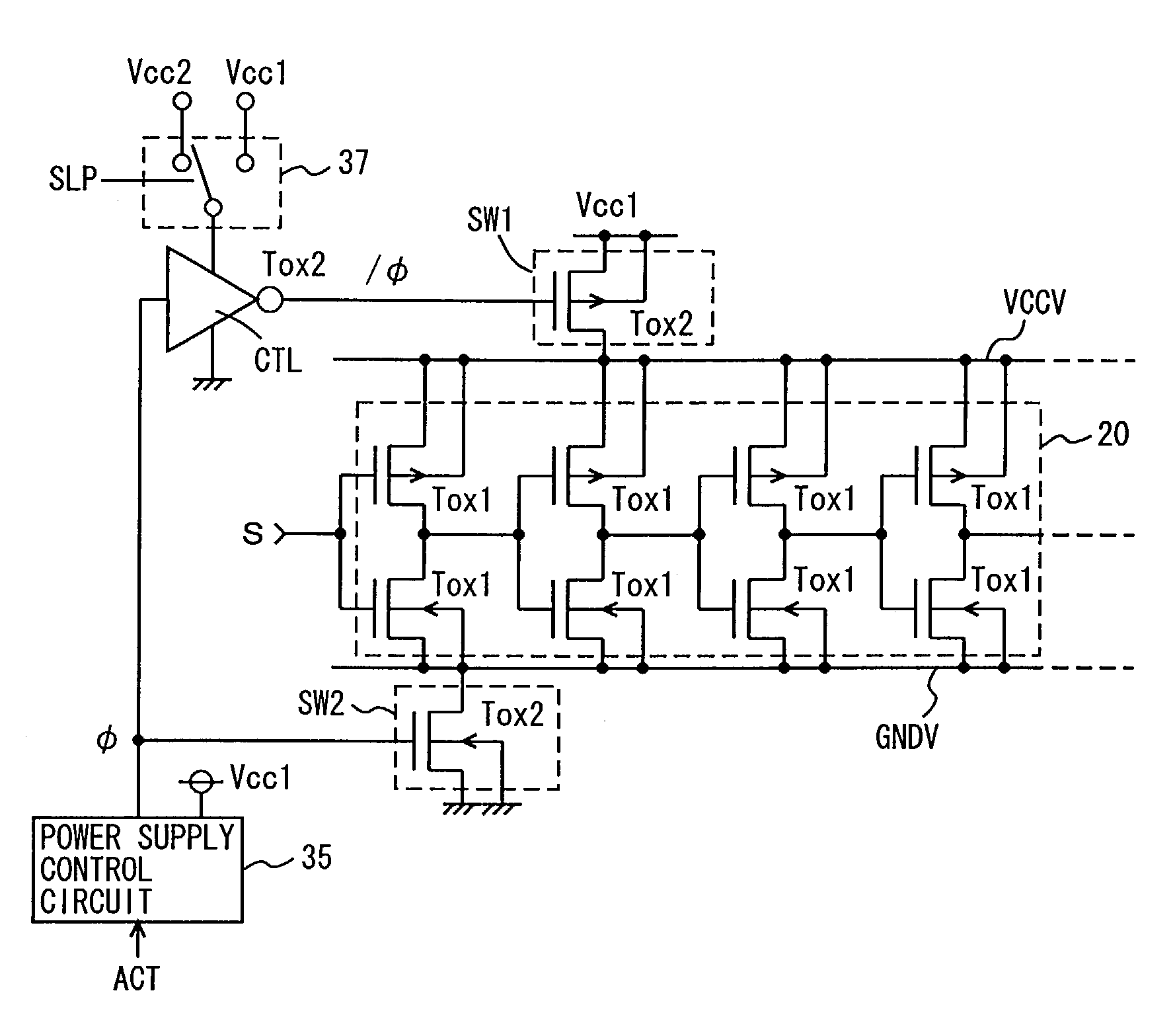
[0073]FIG. 1 shows a configuration of a semiconductor device according to the present invention in a first embodiment. In FIG. 1, the semiconductor device includes, as an internal function circuit, CMOS inverters IV1 to IV4 cascaded in four stages by way of example. CMOS inverters IV1 to IV4 each include a p channel MIS transistor PT and an n channel MIS transistor NT. MIS transistors PT and NT each have a gate insulation film having a thickness Tox1, for example, of 2 nm.
[0074]The p channel MIS transistors of CMOS inverters IV1 to IV4 have their respective sources and substrate regions (or backgates) connected commonly to a high-side virtual power source line (hereinafter simply referred to as a virtual power supply line) VCCV. The n channel MIS transistors of CMOS inverters IV1 to IV4 have their respective sources and substrate regions connected commonly to a low-side virtual power source line (hereinafter simply referred to as a virtual ground line) GNDV.
[0075]Virtual power ...
first modification
[0101
[0102]FIG. 6 shows a configuration of the semiconductor device of a first modification of the first embodiment. In the configuration of FIG. 6, in control circuit 5 generating switch control signals φ and / φ, there are provided an inversion circuit CTL1 having a level conversion function and receiving a mode instructing signal φFB, and a CMOS inverter CTL2 receiving a signal from inversion circuit CTL1 to generate switch control signal / φ.
[0103]Inversion circuit CTL1 and CMOS inverter CTL2 receive power supply voltage Vcc2 and a negative voltage VBB as operating power supply voltages. Therefore, switch control signals φ and / φ changes between the voltage Vcc2 and negative voltage VBB.
[0104]Negative voltage VBB is generated from a VBB generation circuit 15 receiving power supply voltage Vcc2 to generate negative voltage VBB through, for example, a charge pumping operation. Power supply voltage Vcc2 is generated from external power supply voltage EXVcc2 supplied to power supply n...
second embodiment
[0113
[0114]FIG. 8 shows a configuration of the semiconductor device according to a second embodiment of the present invention. The semiconductor device shown in FIG. 8 includes, in addition to the configuration of the semiconductor device shown in FIG. 1, a power supply switch circuit SW3 provided between a virtual power supply line VCCV and a power supply node receiving power supply voltage Vcc1 and a power supply switch circuit SW4 provided between virtual ground line GNDV and a ground node.
[0115]Power supply switch circuit SW3 is constructed of an n channel MIS transistor NQ1 connected between a power supply node receiving power supply voltage Vcc1 and virtual power supply line VCCV, and having its gate receiving switch control signal φ and its backgate connected to a ground node. N channel MIS transistor NQ1 has a gate insulation film of thickness Tox2.
[0116]Power supply switch circuit SW4 is constructed of a p channel MIS transistor PQ1 connected between virtual ground line GND...
PUM
 Abstract
Description
Claims
Application Information