Light emitting element and method for manufacturing the same

a technology of light emitting elements and manufacturing methods, which is applied in the manufacture of electrode systems, multiplex communication, electric discharge tubes/lamps, etc., to achieve the effect of small luminance deterioration and alligatory of luminan

Inactive Publication Date: 2006-06-13
SEMICON ENERGY LAB CO LTD
View PDF22 Cites 16 Cited by
  • Summary
  • Abstract
  • Description
  • Claims
  • Application Information

AI Technical Summary

Benefits of technology

[0020]By carrying out the invention, it is possible to fabricate a light emitting element which alleviates deterioration of luminance. Also, by using the such improved light emitting element, it is possible to provide a light emitting device in

Problems solved by technology

Further, a problem addressed is in providing an electronic equipment

Method used


Image

  • Light emitting element and method for manufacturing the same
  • Light emitting element and method for manufacturing the same
  • Light emitting element and method for manufacturing the same

Examples


embodiment 1

[Embodiment 1]

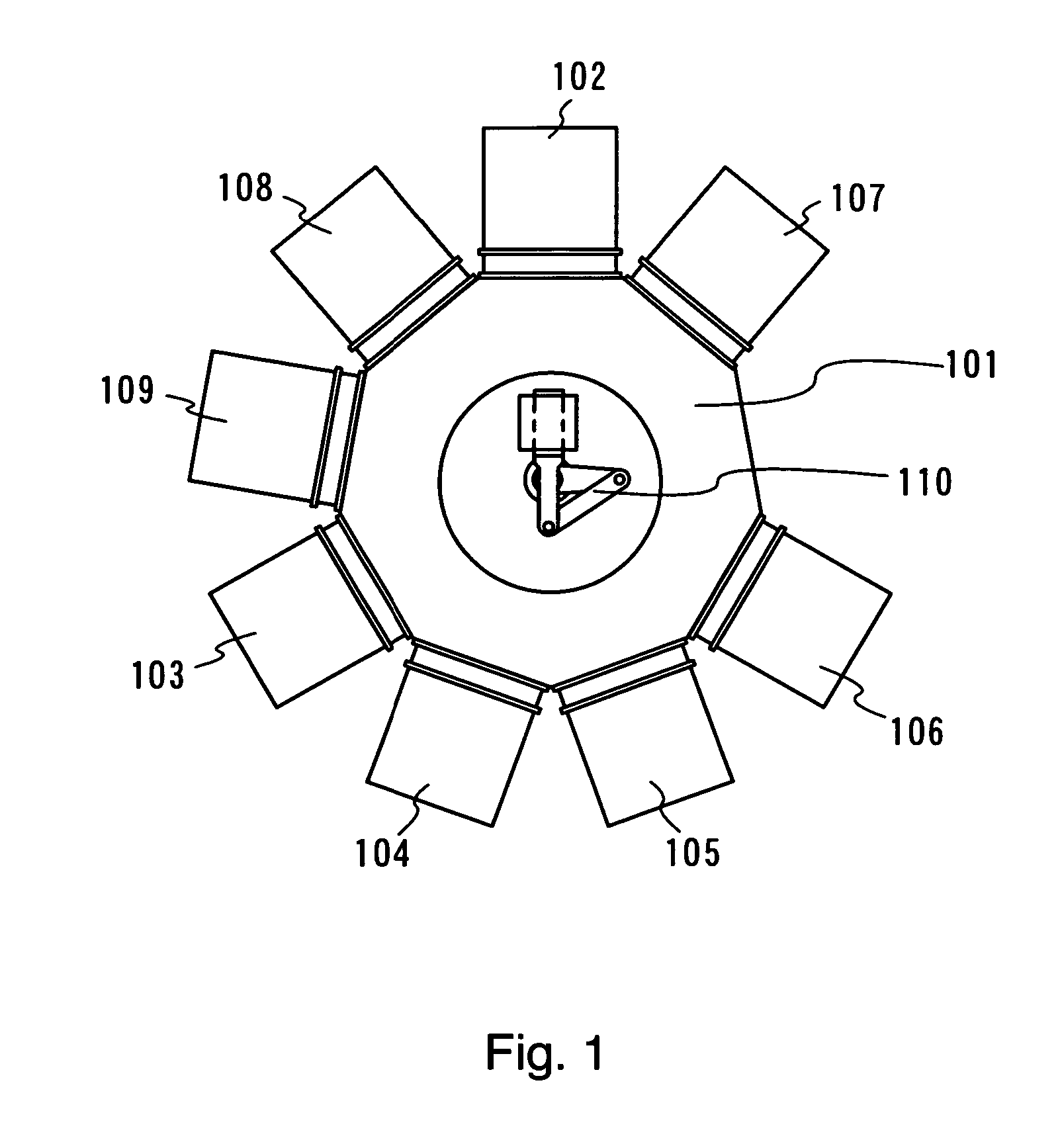
[0035]In this embodiment, a process of making a light emitting element in accordance with the invention is disclosed, and a manufacturing device of a multi-chamber system which is used is described. This manufacturing device can carry out sealing processing by uniting with an opposing substrate, which is cast in separately from a substrate, after the substrate is cast in, and processing of film formation etc. is carried out continuously.

[0036]A light emitting element manufacturing device shown in FIG. 1 has a transport chamber 101 (a substrate and an opposing substrate, a transport robot 110 for transporting a metal mask are attached), a substrate / mask stock chamber 102 which is coupled to the transport chamber through a gate valve, a preprocessing chamber 103, an organic deposition chamber 1104, an organic deposition chamber 2105, a metal deposition chamber 106, a CVD chamber 107, a sealing glass stock chamber 108, and a sealing chamber 109.

[0037]In the first place, c...

embodiment 2

[Embodiment 2]

[0057]In this embodiment, in the light emitting element which was fabricated by the processes shown in the embodiment 1, luminance deterioration was measured on the occasion that constant current drive was carried out.

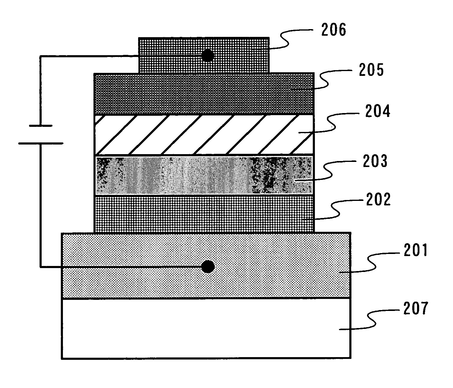
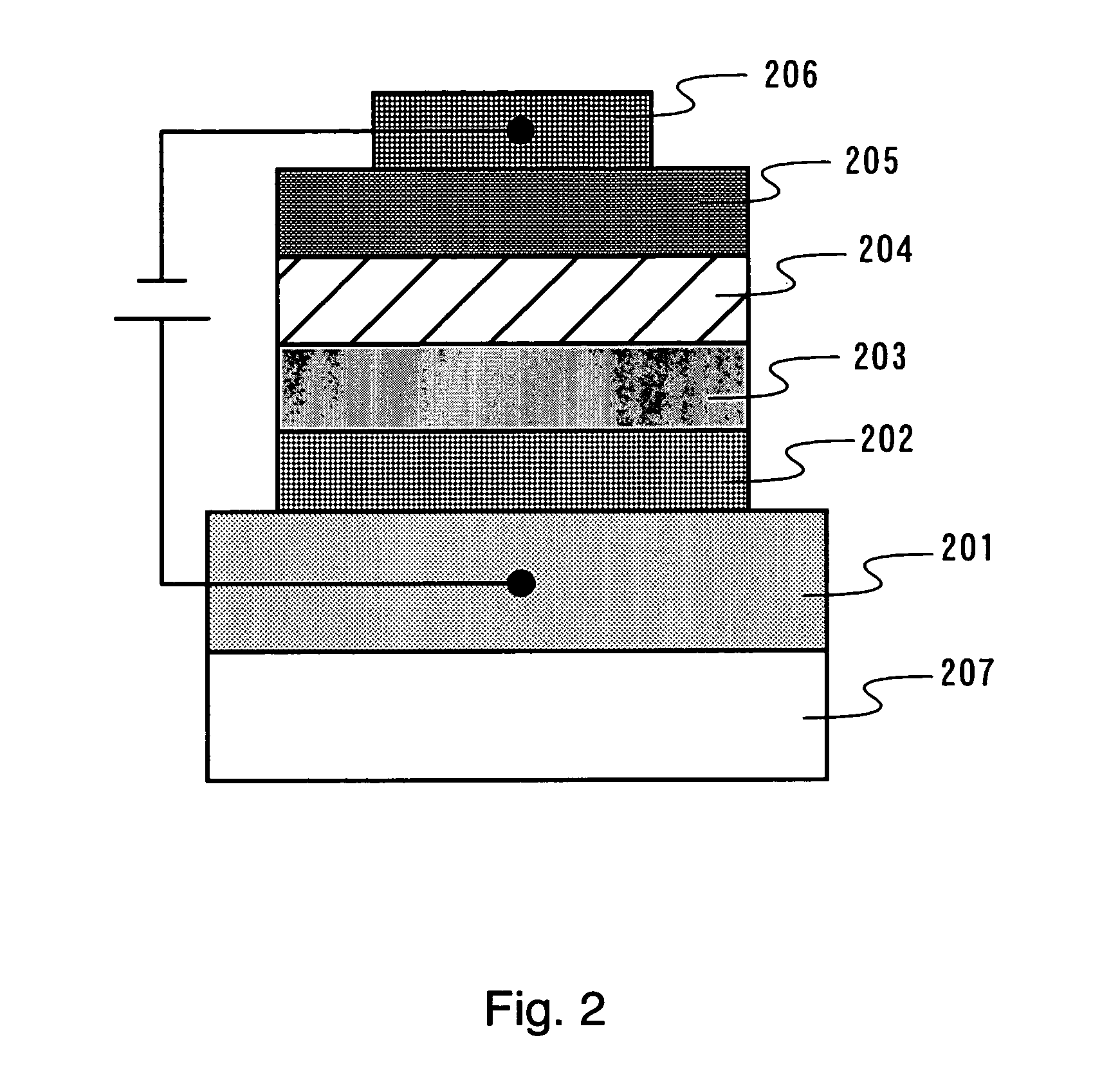
[0058]An element structure is shown in FIG. 2. Firstly, after CuPc as a hole injection layer 202 was deposited by 20 nm in vacuum of 10−5–10−6 Pa, to a glass substrate 207 on which a film of ITO of 110 nm was formed as an anode 201, it is exposed for 5 minutes in oxygen gas atmosphere. After that, as a hole transport layer 203, NPB was deposited by 60 nm. As a light emitting layer 204, a co-deposition film of Alq and DMQA was deposited by 37.5 nm. As an electron transport layer 205, Alq was deposited by 37.5 mm. Then, as a cathode 206, CaF2 and Al were deposited by 1 nm and 200 nm, respectively. A mass ratio of Alq and DMQA was 1:0.003. Then, it is glued together with an opposing glass with a dry agent, to which ultraviolet cured resin was applied, and ul...

embodiment 3

[Embodiment 3]

[0061]In this embodiment, by slightly changing an element structure of the embodiment 2, constant current reliability of an element was measured. In the embodiment 2, a mass ratio of a light emitting layer is 1:0.003 between Alq and DMQA, whereas in this embodiment, it is made to be 1:0.01. Other element structures and an element manufacturing method were identical. Initial luminance was 1000 cd / m2. Current density which corresponds to this was 13.4 mA / cm2. It is shown in “oxygen atmosphere presence”.


PUM


Abstract

In order to provide a light emitting device and an electronic equipment which suppress luminance deterioration, and have long life, the invention does not form an organic compound layer which is composed of a hole injection layer, a hole transport layer, a light emitting layer, an electron transport layer, an electron injection layer and so on, and electrodes in vacuum-through, as in a conventional vacuum deposition method, but after a hole injection layer, which comprises phthalocyanine, is formed, it is exposed to gas atmosphere. In particular, copper phthalocyanine is exposed to oxygen atmosphere. By this method, provided is an organic light emitting element which has long life, and by using the above-described organic light emitting element, a light emitting device and an electronic equipment are fabricated.

Description

TECHNICAL FIELD[0001]This invention relates to a manufacturing method of a light emitting element which can obtain fluorescence or phosphorescence, by applying an electric field to such an element that a film including an organic compound (hereinafter, inscribed as “organic compound layer”), is disposed between a pair of electrodes.BACKGROUND OF THE INVENTION[0002]A light emitting element is a element which emits light by applying an electric field. As to its light emission mechanism, it is said that by applying a voltage to electrodes, and interposing an organic compound layer therebetween, electrons which are injected from a cathode and holes which are injected from an anode, are recombined at a light emission center in an organic compound layer to form molecules which are in an excitation state (hereinafter, inscribed as “molecular exciter”), and the molecular exciter discharges energy to emit light on the occasion of returning to a ground state.[0003]As types of molecular excite...

Claims


Application Information

Patent Timeline
IPC IPC(8): H04J9/00H01J9/24H01J9/00H01L51/00H01L51/30H01L51/40H01L51/50H05B33/10
CPCH01L51/001H01L51/5088H01L51/0078H01L51/5052H10K71/164H10K85/311H10K50/155H10K50/17
Inventor IKEDA, HISAO
Owner SEMICON ENERGY LAB CO LTD
Why Eureka
Try Eureka