Narrow width effect improvement with photoresist plug process and STI corner ion implantation

a photoresist plug and narrow width technology, applied in semiconductor/solid-state device manufacturing, semiconductor devices, electrical equipment, etc., can solve the problems of reducing threshold voltage (vt), affecting the performance and reliability of nmos transistors, and reducing the vt of nmos transistors, so as to reduce the tendency to migrate, improve the vt roll-off effect, and mitigate the effect of localized electrical fields

Inactive Publication Date: 2006-07-04
TAIWAN SEMICON MFG CO LTD
View PDF12 Cites 39 Cited by
  • Summary
  • Abstract
  • Description
  • Claims
  • Application Information

AI Technical Summary

Benefits of technology

[0012]One objective of the present invention is to provide a means of improving the reverse narrow width effect without degrading isolation and junction leakage.
[0013]A further objective of the present invention is to provide a method of improving NMOS narrow width Vt roll-off with high flexibility.
[0014]A still further objective of the present invention is to achieve an improvement in reverse narrow width effect without implementing new equipment that will drive up the cost of fabrication.
[0016]The advantage of the indium implant is that the indium dopant has a lower tendency to migrate than boron and serves to mitigate the effect of the localized electrical field that is induced by the presence of the gate layer in the grooves formed within the insulator layer at top corners of the shallow trench.
[0017]The present invention is also a semiconductor device comprising an NMOS transistor that includes a substrate having an active region formed between shallow trench isolation structures. Each shallow trench has an oxide liner along its sidewalls and bottom and is filled with an insulator material to a level above the substrate. A gate dielectric layer covers the active region and a patterned gate layer is formed on the gate dielectric layer. An indium dopant is located near the surface of the substrate in a region that abuts the top corners of the shallow trench. Other p-type dopants may be present at the surface of the substrate in the active region but the total concentration of dopants is highest in the indium doped regions. This device is especially useful in improving NMOS Vt roll-off for transistors having a channel length of about 1 micron or less.

Problems solved by technology

One particular problem with devices having a channel length smaller than about 1 micron is referred to as a reverse narrow width effect in which threshold voltage decreases as the width of a shallow trench isolation (STI) feature that separates active areas decreases.
As a result, the NMOS transistor performance and reliability are degraded.
The presence of this conducting material can induce a local electric field below the corners of the gate oxide in the final device which leads to a lower threshold voltage (Vt) and higher leakage current in the NMOS transistor.
However, P+ to P well isolation is expected to be degraded due to the boron implant compensating the N well at the STI sidewall.
Since the implant is performed prior to high temperature oxidation and anneal steps in the trench fabrication, a considerable amount of dopant is likely to be lost from the implanted regions.
The method teaches that the lower mobility of indium compared with boron in a substrate results in a lower threshold voltage skew but does not address the influence of the etched recess in an STI structure on reverse narrow width effect in an NMOS transistor which may also be referred to as Vt roll-off.
Furthermore, the method does not allow for a higher dopant concentration in a region of the substrate adjacent to the STI corners and a lower concentration in other parts of the active region.
However, the method does not address the problem of Vt roll-off caused by an etched recess at top corners of the STI structure.

Method used


Image

  • Narrow width effect improvement with photoresist plug process and STI corner ion implantation
  • Narrow width effect improvement with photoresist plug process and STI corner ion implantation
  • Narrow width effect improvement with photoresist plug process and STI corner ion implantation

Examples


Embodiment Construction

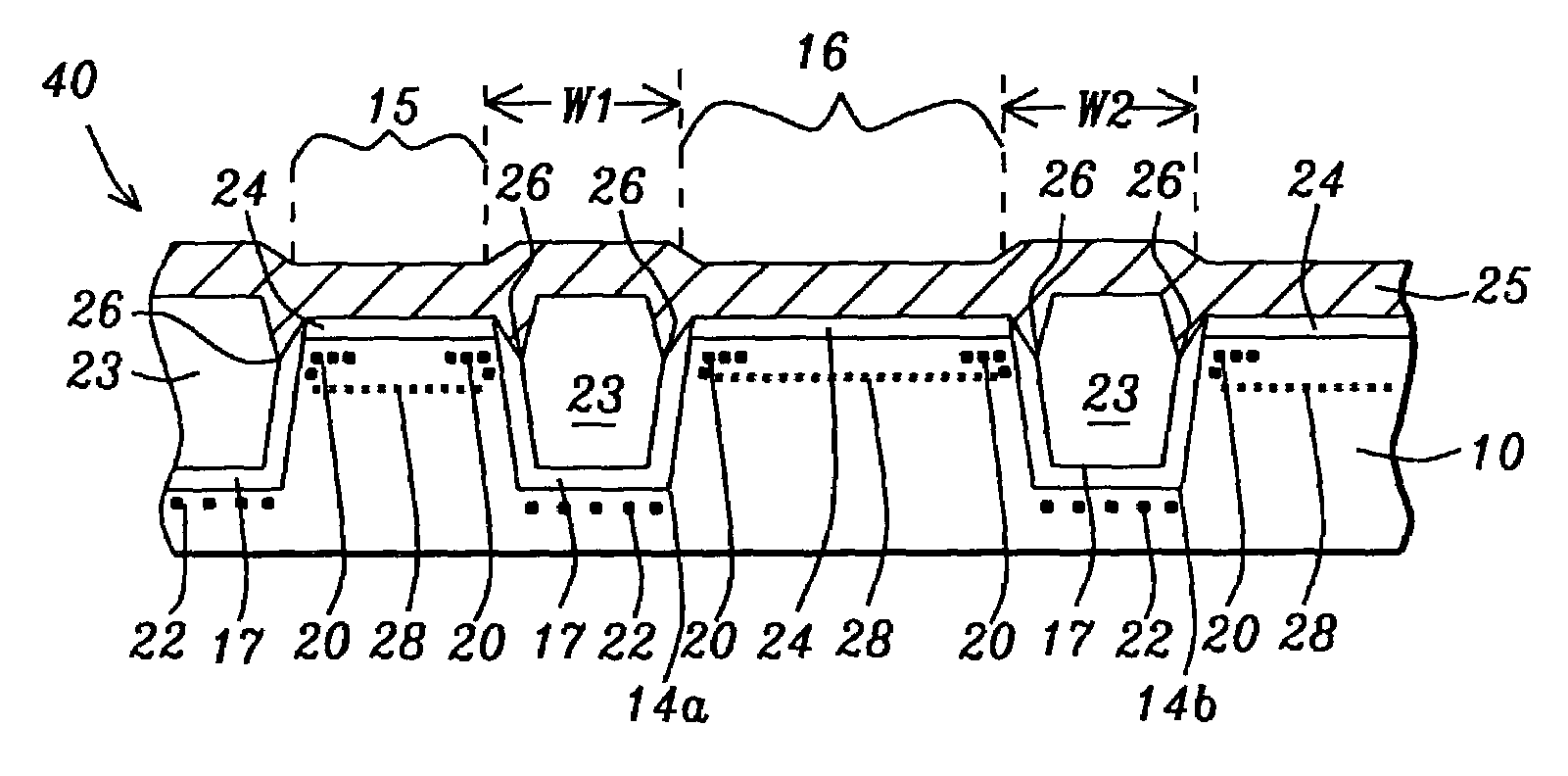
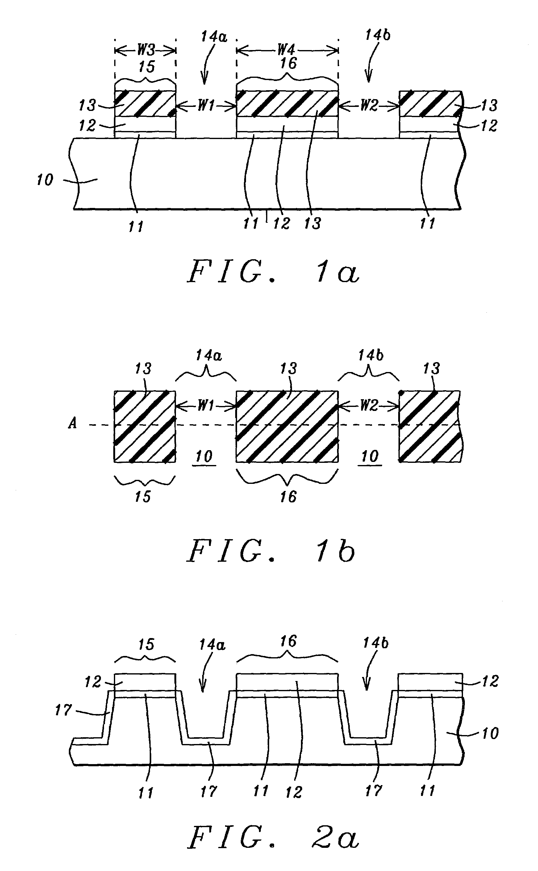
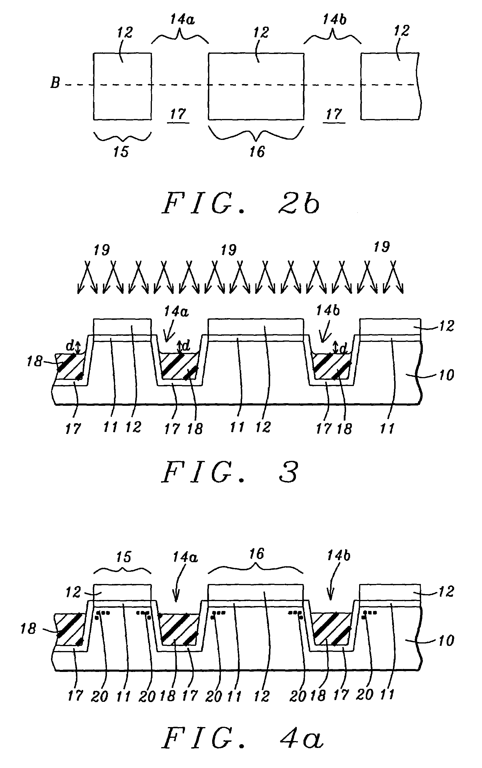
[0029]The present invention is a method of improving the reliability and performance of NMOS transistors in a semiconductor device by improving the Vt roll-off for short channel devices. However, the method is also effective for long channel devices. The invention is not limited to the specific examples described herein and the figures are not necessarily drawn to scale.

[0030]Referring to FIG. 1a, a substrate 10 is provided which is typically silicon but may be based on silicon-on-insulator, silicon-germanium, or gallium-arsenide technology. Furthermore, the substrate 10 may be doped or undoped. A pad oxide layer 11 is formed on substrate 10 and has a thickness in the range of about 30 to 200 Angstroms. A cap layer 12 which is preferably silicon nitride is then deposited on pad oxide 11 by a chemical vapor deposition (CVD) or plasma enhanced CVD technique. Cap layer 12 has a thickness between about 200 and 5000 Angstroms.

[0031]Trenches 14a, 14b are formed by first coating a photores...


PUM


Abstract

A method to reduce the inverse narrow width effect in NMOS transistors is described. An oxide liner is deposited in a shallow trench that is formed to isolate active areas in a substrate. A photoresist plug is formed in the shallow trench and is recessed below the top of the substrate to expose the top portion of the oxide liner. An angled indium implant through the oxide liner into the substrate is then performed. The plug is removed and an insulator is deposited to fill the trenches. After planarization and wet etch steps, formation of a gate dielectric layer and a patterned gate layer, the NMOS transistor exhibits an improved Vt roll-off of 40 to 45 mVolts for both long and short channels. The improvement is achieved with no degradation in junction or isolation performance. The indium implant dose and angle may be varied to provide flexibility to the process.

Description

FIELD OF THE INVENTION[0001]The invention relates to a method of fabricating an integrated circuit in a semiconductor device. More particularly, the present invention relates to the formation of an NMOS transistor comprising a shallow trench isolation structure.BACKGROUND OF THE INVENTION[0002]As design rules shrink for MOSFET (Metal Oxide Semiconductor Field Effect Transistor) devices, there is a need to improve the reliability and performance of n-type (hereafter called NMOS) transistors. One particular problem with devices having a channel length smaller than about 1 micron is referred to as a reverse narrow width effect in which threshold voltage decreases as the width of a shallow trench isolation (STI) feature that separates active areas decreases. As a result, the NMOS transistor performance and reliability are degraded.[0003]A conventional process for fabricating a NMOS transistor involves forming a pad oxide on a substrate and depositing a silicon nitride cap layer on the p...

Claims


Application Information

Patent Timeline
Patent Type & Authority Patents(United States)
IPC IPC(8): H01L29/76H01L29/94H01L31/062H01L31/113H01L31/119H01L21/762H01L21/8234
CPCH01L21/823481H01L21/76237H01L21/26586
Inventor SHEU, YI-MINGLIN, DA-WENCHEN, CHENG-KUYEH, PO-YINGPENG, SHI-SHUNGWU, CHUNG-CHENG
Owner TAIWAN SEMICON MFG CO LTD
Why Eureka
Try Eureka