Electronic device

a technology of electronic devices and components, applied in the field of electronic devices, to achieve the effect of high melting point of intermetallic compounds, sufficient bonding strength, and sufficient bonding strength

Inactive Publication Date: 2006-07-11
RENESAS ELECTRONICS CORP
View PDF39 Cites 19 Cited by
  • Summary
  • Abstract
  • Description
  • Claims
  • Application Information

AI Technical Summary

Benefits of technology

[0025]For example, regarding temperature-hierarchical bonding, even when a part of solder on the higher-temperature side that has already been bonded melts, the solder can provide strength high enough to withstand a process during later solder bonding if other portion does not melt.
[0026]The melting points of intermetallic compounds are high. Because portions bonded with intermetallic compounds can provide sufficient bonding strength even at 300° C., intermetallic compounds can be used for temperature-hierarchical bonding on the higher-temperature side. Therefore, the present inventors performed bonding by use of a paste which is a mixture of Cu (or Ag, Au, Al or plastic) balls or these balls whose surfaces are plated with Sn, etc. and Sn-base solder balls, both of them being mixed at a volume ratio of about 50% to about 50%. As the result, in portions where the Cu balls are in contact with each other or in close vicinity to each other, a reaction with surrounding molten Sn occurs and a Cu6Sn5 intermetallic compound is formed because of diffusion between Cu and Sn, making it possible to ensure sufficient bonding strength between the Cu balls at high temperatures. Because the melting point of this compound is high and sufficient strength is ensured at a soldering temperature of 250° C. (only the Sn portion melts), no exfoliation of bonded portions occurs during secondary reflow performed for mounting onto a printed circuit board. Therefore, the soldered portions of a module are made of a composite material having two functions, that is, the first function of ensuring high-temperature strength during the secondary reflow by elastic bonding force brought about from the bonding of the high-melting point compound and the second function of ensuring service life by the flexibility of soft Sn during temperature cycles. Therefore, the soldered portions can be adequately used in the temperature-hierarchical bonding at the high temperatures.
[0027]Furthermore, also in the case of hard and high-rigidity solders having desirable melting points, such as an Au-20Sn solder, Au-(50–55)Sn solders (melting point: 309–370° C.) and an Au-12Ge (melting point: 356° C.), by using granular particles and dispersing and mixing soft and elastic rubber particles or by dispersing and mixing soft low-melting point solders of Sn, In, etc. among the above hard and high-rigidity solders, it is possible to ensure bonding strength even at temperatures of not less than the solidus temperatures of the above hard and high-rigidity solders and to relieve phenomena caused due to deformation, by the soft Sn, In or rubber among metal particles, whereby such a new effect as to compensate for the drawbacks of solders can be expected.

Problems solved by technology

Specifically, problems in the results of an evaluation of an RF (radio frequency) module are stated below.

Method used


Image

  • Electronic device
  • Electronic device
  • Electronic device

Examples


embodiment 1

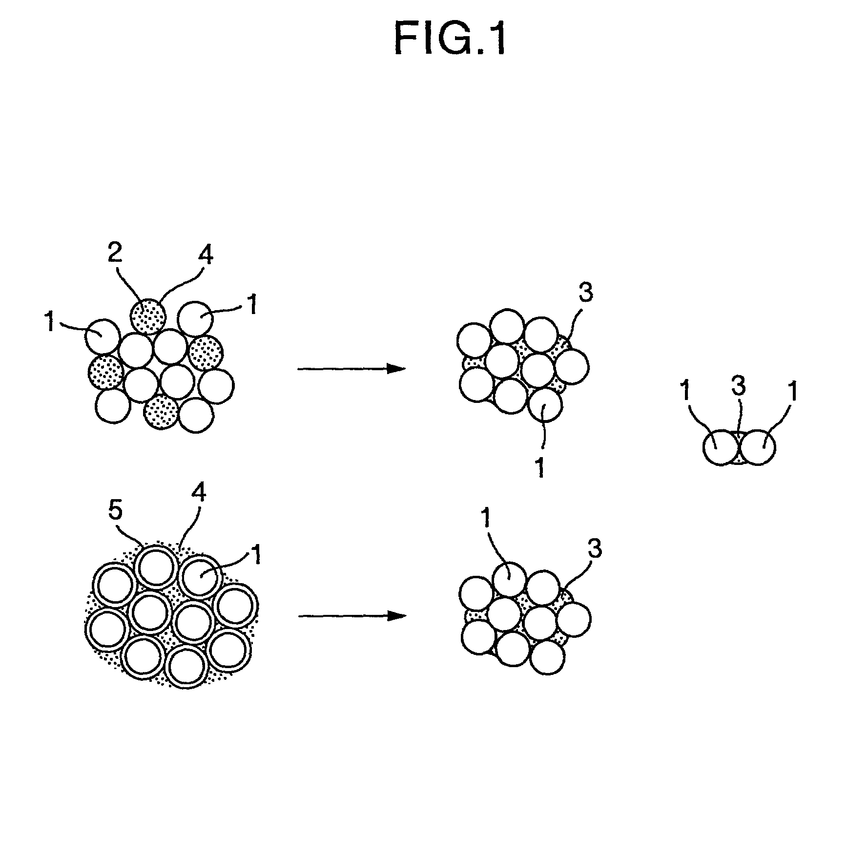
[0052]FIG. 1 shows the concept of a bonding structure relating to the invention. This figure also shows a condition before soldering and another condition after soldering. The upper portions of FIG. 1 shows an example of use of a paste in which Cu balls 1 with a particle size of about 30 μm (or balls of Ag, Au, Cu—Sn alloys, etc., or those to which an Au plating, and Ni / Au plating, etc., are applied, or those to which an Sn plating, etc., are applied) and Sn solder balls 2 (melting point: 232° C.) with a particle size of about 30 μm are appropriately dispersed in small quantities via a flux 4. When this paste is subjected to reflow at a temperature of not less than 250° C., the Sn solder balls 2 melt, molten Sn 3 spreads so that it wets the Cu balls 1 and becomes present between the Cu balls 1 relatively uniformly. The Cu balls need not be spherical; that is, Cu balls having great surface irregularities, bar-like ones, and those containing dendrite crystals may be used. In this case...

embodiment 2

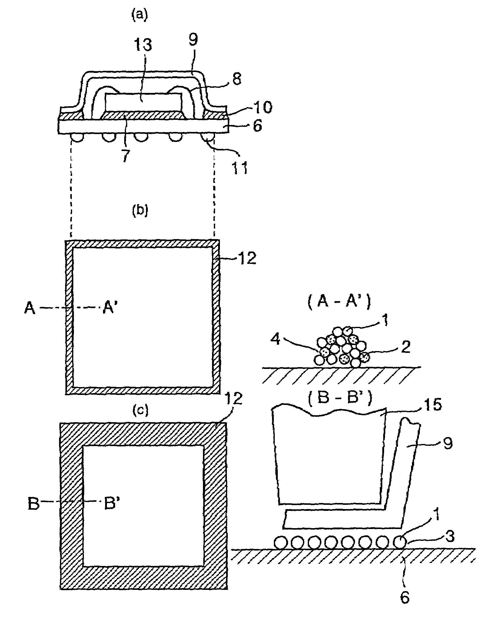
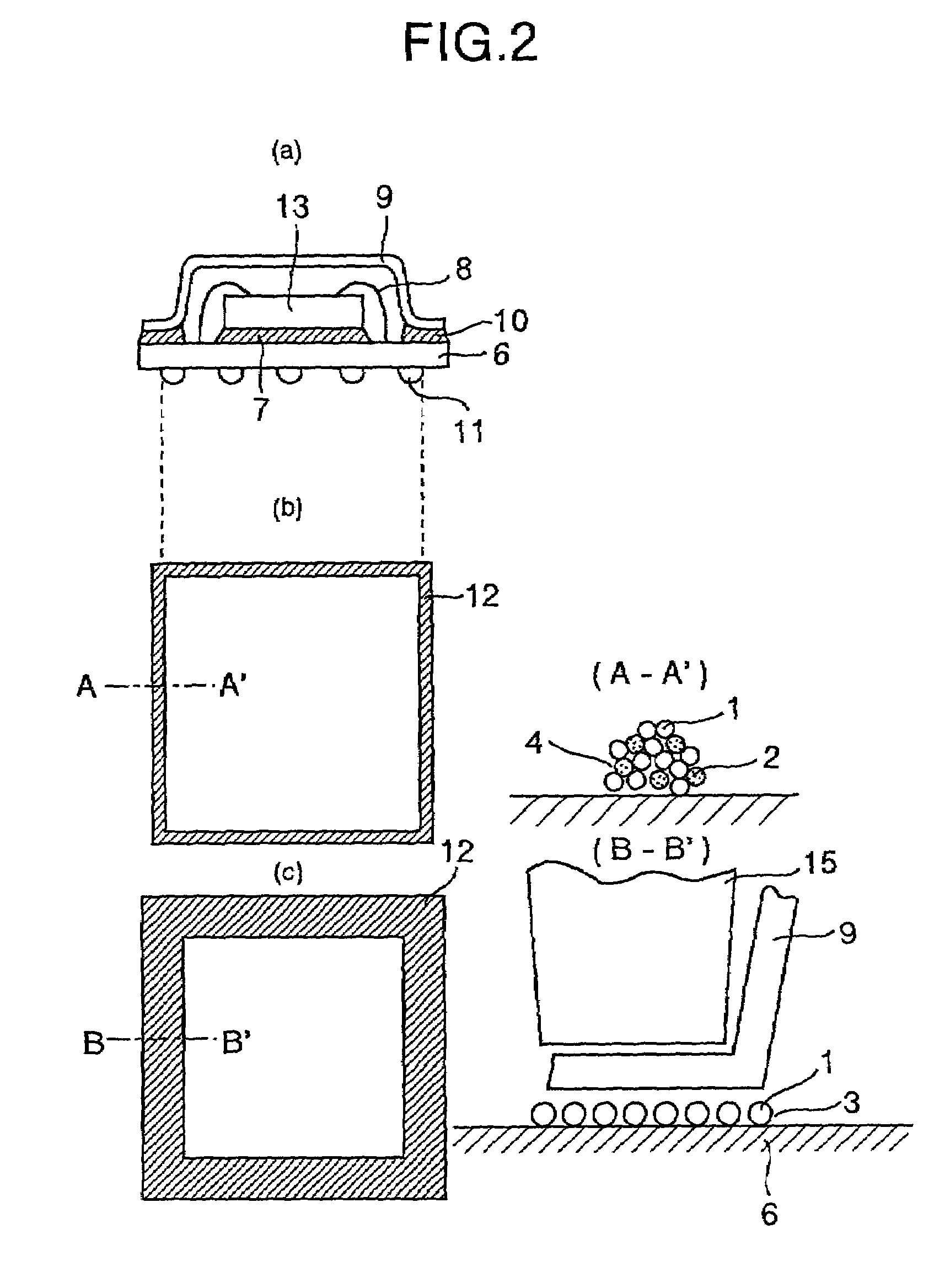
[0057]In FIG. 2(a), a semiconductor device 13 is bonded to a junction substrate 6 by use of an Au-20Sn solder, etc. and after wire bonding 8, the peripheral portion of a cap 9, which is fabricated by plating Al, Fe—Ni, etc. with Ni—Au, is bonded 10 to the junction substrate by reflow through the above solder paste of non-cleaning type. On this occasion, when the insulating characteristic is regarded as important, it is desirable to perform bonding in a nitrogen atmosphere by use of a solder with a flux not containing chlorine. However, when the wettability cannot be ensured, the encapsulation with a weak-activity rosin of RMA type may be performed. This semiconductor device is not required to have a perfect encapsulatability and, therefore, if the flux has adequate insulating characteristics, there occurs no influence of holding for a long time on the semiconductor device even in the presence of the flux. The purpose of the cap encapsulation is mainly mechanical protection. As a met...

embodiment 3

[0063]The paste relating to the invention can also be used in the die bonding 7 shown in FIG. 2(a). After bonding by use of the paste relating to the invention, cleaning and wire bonding are performed. In prior arts, the die bonding is performed by use of an Au-20Sn solder, however, it has been limited to small chips in view of reliability. Also, in the case of Pb-base solders, a Pb-10Sn solder, etc., have been used. The bonding relating to the invention can be used even in chips having a somewhat larger area. The larger the thickness of a bonding portion, the longer the service life and the higher the reliability become. In the invention, it is possible to make this thickness larger by using high melting point balls each having a larger size. In a case of making this thickness small, this is performed by making the size of particles (, that is, balls) small. In some bonding methods, it is also possible to use a thin bonding portion by reducing the particle size. Even Cu particle si...


PUM

PropertyMeasurementUnit
diameteraaaaaaaaaa
melting pointaaaaaaaaaa
temperaturesaaaaaaaaaa

Abstract

Each of junctions formed between a semiconductor device and a substrate comprises metal balls of Cu etc. and compounds of Sn and the metal balls, and the metal balls are bonded together by the compounds.

Description

CROSS REFERENCE TO RELATED APPLICATION[0001]This application claims priority from Japanese Application No. 2000-180719, filed Jun. 12, 2000 and from Japanese Application No. 2000-396905, filed Dec. 25, 2000.BACKGROUND OF THE INVENTION[0002]The present invention relates to a technique for performing solder bonding through the use of a temperature hierarchy effective in the module mounting of electronic devices, etc.[0003]In Sn—Pb-base solders, soldering has so far been performed by temperature-hierarchical bonding in which parts are soldered first at temperatures between 330° C. and 350° C. by use of high-temperature solders, such as Pb-rich Pb-5 mass % Sn (hereinafter the indication of “masss %” is omitted and only a numeral is recited) solders (melting point: 314–310° C.) and Pb-10Sn solders (melting point: 302–275° C.), and bonding is then performed with the aid of Sn-37Pb eutectics (183° C.) of a low-temperature solder without melting soldered portions. This temperature-hierarchi...

Claims


Application Information

Patent Timeline
Patent Type & Authority Patents(United States)
IPC IPC(8): H01L29/40B23K1/00B23K3/06B23K35/14B23K35/22B23K35/24B23K35/26B23K35/28B23K35/30B23K101/40C22C5/02C22C5/06C22C9/02C22C13/00C22C28/00H01L21/50H01L21/52H01L21/56H01L21/60H01L23/10H01L23/12H01L23/31H01L23/36H01L23/367H01L23/433H01L23/485H01L23/492H01L23/495H01L23/50H05K1/14H05K3/34
CPCH05K3/3484B32B15/01C22C5/02C22C9/02C22C11/06C22C13/00H01L21/50H01L21/56H01L21/563H01L23/10H01L23/3128H01L23/3677H01L23/4334H01L23/4924H01L23/49513H01L24/11H01L24/16H01L24/29H01L24/81H01L24/83H01L24/97H01L25/16H01L24/13H01L24/32H01L2924/01074H01L2924/01075H01L2924/01078H01L2924/01079H01L2924/01082H01L2924/01088H01L2924/01322H01L2924/01327H01L2924/09701H01L2924/10253H01L2924/10329H01L2924/13091H01L2924/14H01L2924/15153H01L2924/1517H01L2924/15311H01L2924/16152H01L2924/16315H01L2924/166H01L2924/18301H01L2924/19041H01L2924/19043H01L2924/19105H05K1/141H05K3/3463H05K2201/0215H05K2201/045H05K2201/10636H01L24/45H01L24/48H01L2224/1134H01L2224/1147H01L2224/13099H01L2224/13139H01L2224/13144H01L2224/13147H01L2224/29298H01L2224/32225H01L2224/32245H01L2224/45144H01L2224/48091H01L2224/48227H01L2224/48247H01L2224/49171H01L2224/73203H01L2224/73265H01L2224/81054H01L2224/81203H01L2224/81205H01L2224/8121H01L2224/81409H01L2224/81815H01L2224/8319H01L2224/83801H01L2224/97H01L2924/01003H01L2924/01005H01L2924/01012H01L2924/01013H01L2924/01014H01L2924/01015H01L2924/01022H01L2924/01029H01L2924/0103H01L2924/01032H01L2924/01046H01L2924/01047H01L2924/01049H01L2924/0105H01L2924/01051H01L2924/01028H01L2924/0132H01L24/49H01L2224/2919H01L2924/01006H01L2924/01024H01L2924/01033H01L2924/01087H01L2924/014H01L2924/0665H01L2224/29101H01L2224/16225H01L2224/73204H01L2224/29111H01L2924/0133H01L2924/0134H01L2224/29294H01L2224/45124H01L2924/15738H01L2924/1576H01L2224/13111H01L2224/81024H01L2924/00013H05K2201/09572H01L2224/0401H01L2224/11334H01L2224/06102H01L2224/16235H01L2924/00014H01L2224/85H01L2224/83H01L2924/00H01L2924/00012H01L2924/01031H01L2924/01026H01L2924/3512H01L2924/00015H01L2224/29099H01L2224/29199H01L2224/29299H01L2224/2929H01L2924/15787H01L2924/00011H01L2924/12042H01L2924/181H01L24/73H01L2224/10135H01L2224/81139H01L2224/023H05K3/3485Y02P70/50H01L2224/83205H01L2924/0001B23K35/26
Inventor SOGA, TASAOSHIMOKAWA, HANAENAKATSUKA, TETSUYAMIURA, KAZUMANEGISHI, MIKIONAKAJIMA, HIROKAZUENDOH, TSUNEO
Owner RENESAS ELECTRONICS CORP
Why Eureka
Try Eureka