[0010]In addition, in two feedback loops, the
loop gain particularly of the amplifier control loop varies due to dispersion or variation in characteristics of constituent components in production and hence stability of the loop decreases, and hence it is difficult to obtain a desired output level in a specified or predetermined period of time. It has been also detected that the
system of the polar loop has a problem that when an output control operation is conducted for the
amplitude modulation in the amplitude control loop, the gain of the amplitude control loop changes to reduce a
phase margin and hence stability of the loop is lowered.
[0011]It is therefore an object of the present invention to improve the modulating precision of a transmission waveform and the spectral re-growth and to sufficiently suppress
noise in a receiving frequency bandwidth in a
wireless communication apparatus such as a portable telephone having a function to conduct
phase modulation and
amplitude modulation.
[0012]Another object of the present invention is to provide a reliable
wireless communication apparatus which prevents degradation in stability of a loop due to variation in a
loop gain caused by dispersion in characteristics of constituent components in production.
[0013]Still another object of the present invention is to provide a reliable wireless communication apparatus which prevents, when an output control operation is conducted for amplitude modulation, degradation in stability of a loop due to decrease in a
phase margin caused by variation in an amplitude control loop gain.
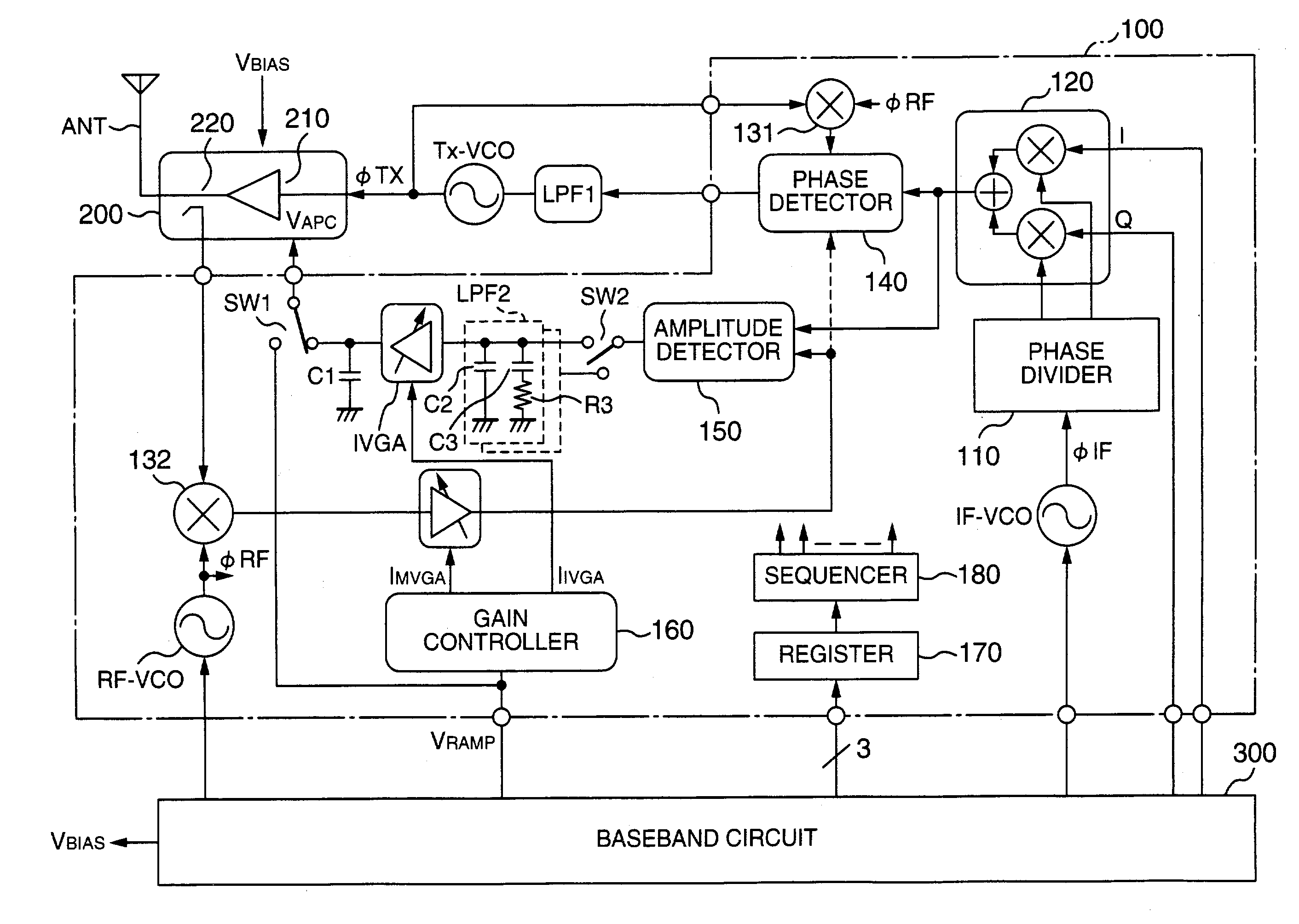
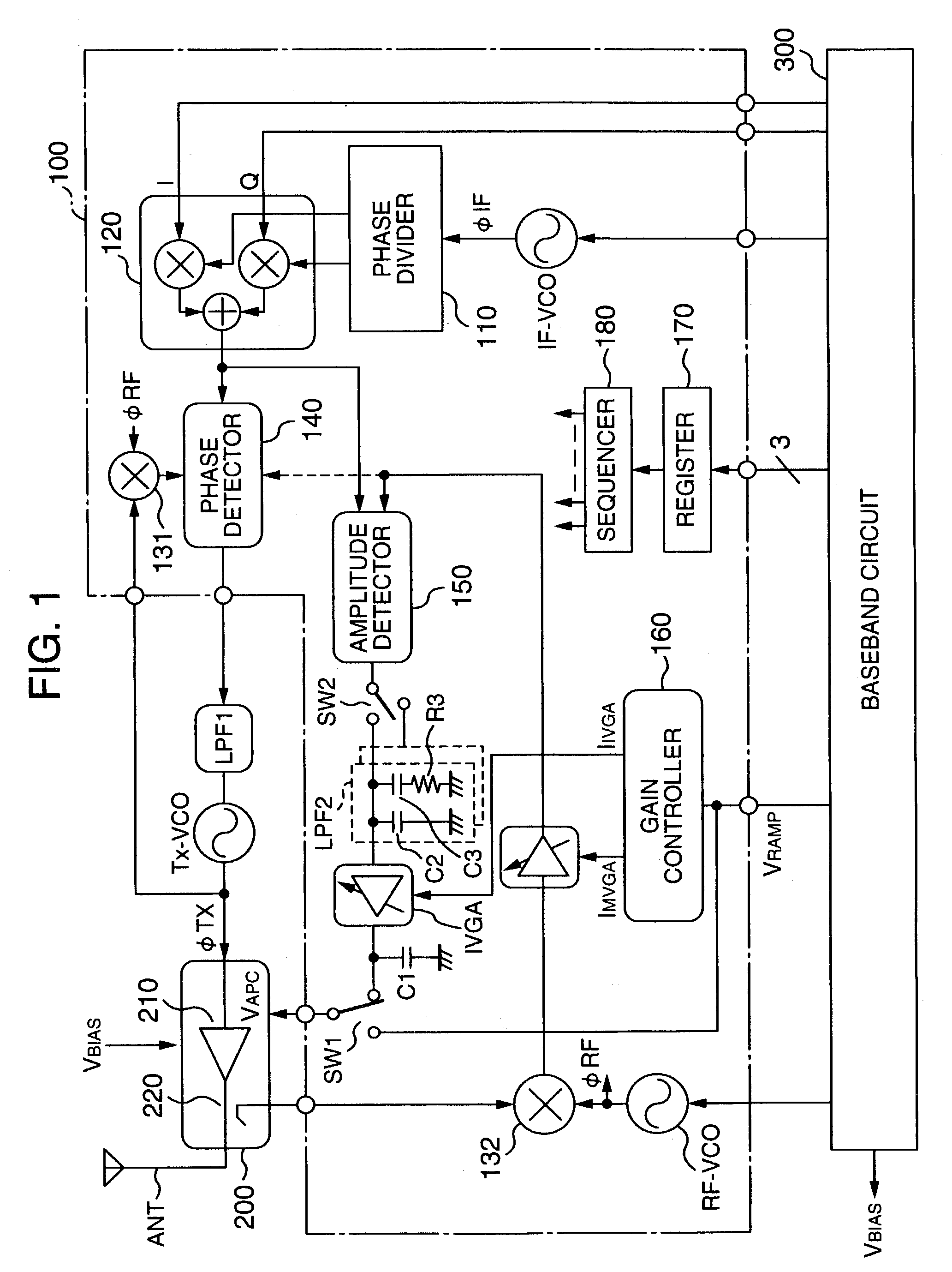
[0015]In a wireless communication apparatus of polar loop type having a
phase control loop to control a phase of a carrier wave or
signal outputted from a transmission oscillator and an amplitude control loop to control amplitude of a transmission output
signal outputted from a power amplifier circuit, there are disposed, on a forward path from an amplifier
detector circuit to a power amplifier circuit which constitute the amplifier control loop, a
variable gain amplifier circuit and a switching unit capable of conducting a change-over of a characteristic of a
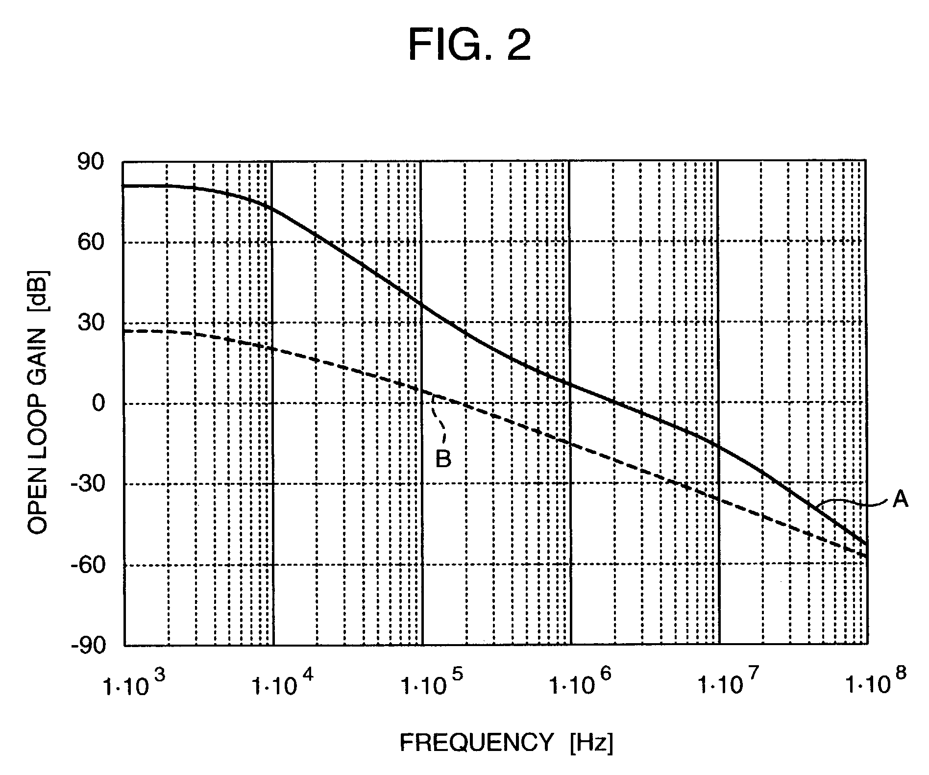
loop filter for a frequency bandwidth of the amplitude control loop to a degree lower than a degree of the filter in an ordinary operation. While the system is being operated in a state in which the
loop filter characteristic is changed to the lower-degree filter characteristic, the output from the power amplifier is measured in this state to calculate variation in the gain of the amplifier loop. According to a result of the calculation, there is obtained data to calibrate or to correct the gain characteristic of the variable gain amplifier circuit with respect to an output
control signal in order to reduce the variation. The correction or corrective data thus obtained is stored in a nonvolatile memory in a
baseband large scale integration (LSI)
chip. Resultantly, by changing the loop filter characteristic to the lower-degree filter characteristic, the measurement can be conducted when the amplitude control loop is in a more
stable state. Additionally, by correcting the gain characteristic of the variable gain amplifier circuit with respect to an output
control signal according to the correction data beforehand measured and stored in the nonvolatile memory, it is possible to calibrate or to correct the variation in the gain of the amplitude control loop caused by the dispersion in characteristics of constituent components in production.
[0016]According to the present invention, there is provided a wireless communication apparatus of polar loop type having a
phase control loop to control a phase of a carrier wave outputted from a transmission oscillator and an amplitude control loop to control amplitude of a transmission output signal outputted from a power amplifier circuit. A variable gain amplifier circuit is disposed in a feedback path from a transmission output level detector circuit to an amplitude detector circuit which constitute the amplitude control loop. A variable gain amplifier circuit is disposed also in a forward path from the amplitude detector circuit to the power amplifier circuit of the loop. Gains of the variable gain amplifier circuits are controlled in mutually opposing directions and the sum of gain of the power amplifier circuit and gain respectively of the variable gain amplifier circuits is controlled to be fixed regardless of the output control signal. As a result, even when the output power is changed, the
open loop gain of the amplitude control loop can be kept fixed. This prevents the degradation of stability of the loop due to the variation or deviation in the loop gain.

