

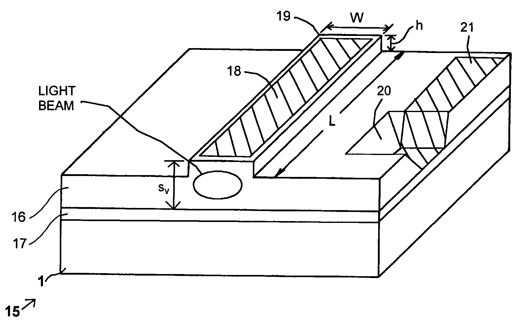
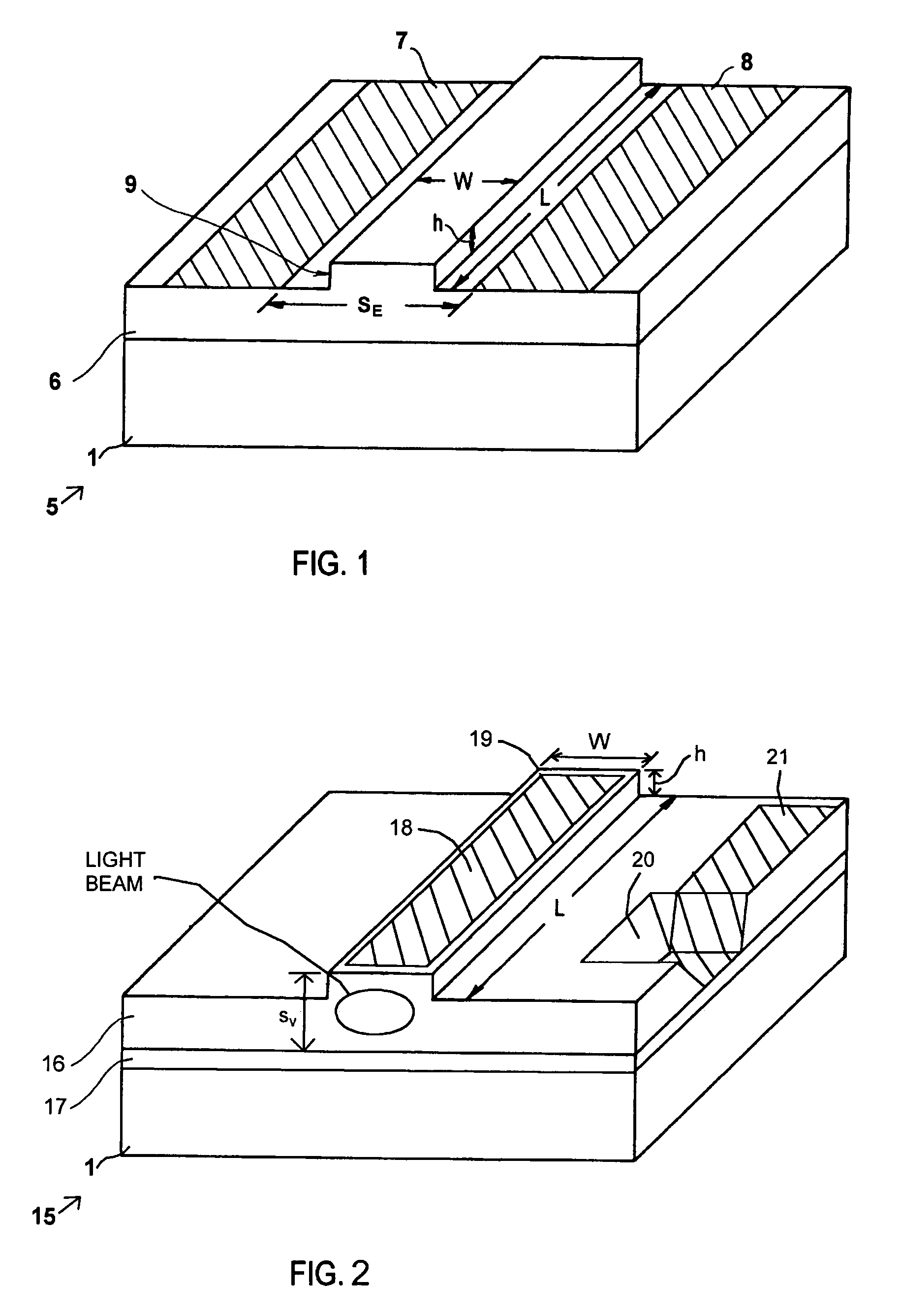
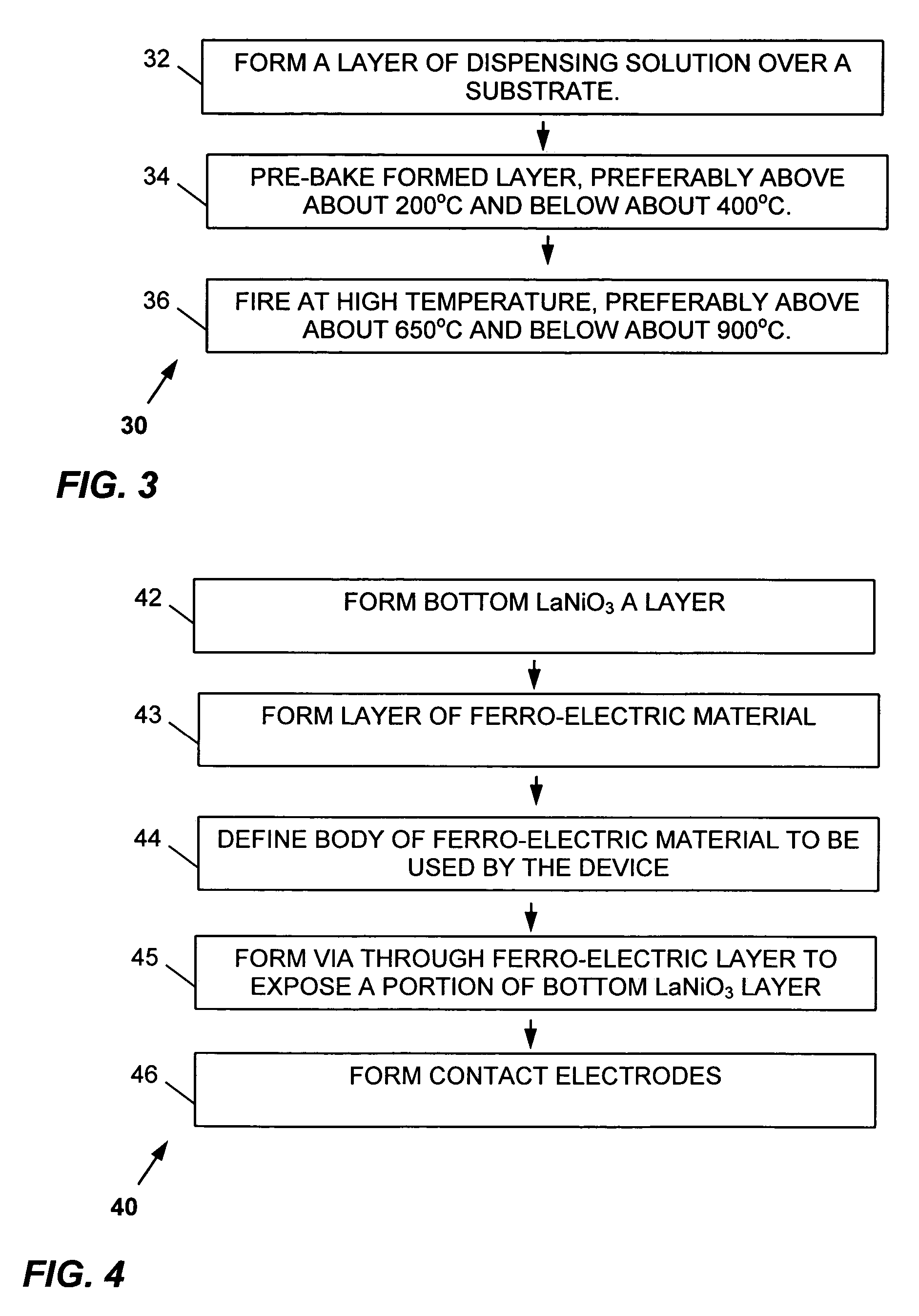
Methods of forming LaNiO3 conductive layers, ferro-electric devices with LaNiO3 layers, and precursor formation solutions
a technology of lanio3 and conductive layers, applied in the field of thin film structures, can solve the problems of reducing the e/o coefficient value of single crystal materials, affecting the e/o coefficient value of lanio3 and the response of single crystal materials to the applied electric field, and the use of crystalline materials in small-scale modulators, etc., to achieve the effect of short spacing distances and higher e/o coefficient values
- Summary
- Abstract
- Description
- Claims
- Application Information
AI Technical Summary
Benefits of technology
Problems solved by technology
Method used
Image

Examples
invention examples 1 and 2
[0041]A first lanthanum nickel oxide sol-gel precursor was prepared by using 1,3-propanediol (diol). Lanthanum acetylacetonate hydrate (Aldrich) and nickel acetate tetrahydrate (98%, Aldrich), in a 1:1 molar ratio to one another, were separately dried at 75° C. for 8 hours under vacuum. FIG. 5 shows the generally accepted general chemical structure (in quasi three-dimensional form) of lanthanum acetylacetonate hydrate before the drying step, where a variable number of water molecules (denoted by “x”) are loosely adhered to parts of the lanthanum acetylacetonate molecule (but not directly to the center lanthanum atom). In the lanthanum acetylacetonate molecule, the lanthanum forms six bonds to six respective acetylacetone groups (molecules). After the drying step, the loosely-adhered water molecules are substantially removed from the lanthanum acetylacetonate molecules.
[0042]FIG. 6 shows the generally accepted general chemical structure of nickel acetate tetrahydrate (in quasi three-...
PUM
| Property | Measurement | Unit |
|---|---|---|
| resistivity | aaaaa | aaaaa |
| surface roughness | aaaaa | aaaaa |
| resistivity | aaaaa | aaaaa |
Abstract
Description
Claims
Application Information