
Charge pump having sampling point adjustment

a charging pump and sampling point technology, applied in the field of communication systems, can solve the problems of high clock speed limiting the usefulness of prior art clock recovery circuits, speed at which high-speed serial transceivers may operate without excessive jitter performance and/or noise performance, and achieve the effect of reducing the number of jitter and noise performance of high-speed serial transceivers

Active Publication Date: 2006-08-15
XILINX INC
View PDF10 Cites 68 Cited by
  • Summary
  • Abstract
  • Description
  • Claims
  • Application Information

AI Technical Summary

Benefits of technology

[0012]The present invention provides for a device and a method for adjusting a sampling point for high-speed serial data. Adjustment circuitry in a charge pump of a phase-locked loop selectively sinks current from an error current produced at a pair of summing points to a loop filter in order to adjust a control voltage of a voltage controlled oscillator (VCO). The adjusted VCO control voltage causes an instantaneous change in a frequency of oscillation of the VCO which is produced to a clock and data recovery (CDR) module as a feedback signal with a phase shift. The change in oscillation frequency causes a relative phase change between the feedback signal and the incoming high-speed serial data thus changing the sampling point of the high-speed serial data.
[0013]A current control module in the adjustment circuitry adjusts a plurality of current mirror devices to sink a ΔI current from one of a positive current summing point and a negative current summing point. The magnitude of the ΔI current that is sinked from the summing points causes the error current produced by the cha

Problems solved by technology

Higher clock speeds limit the usefulness of prior art clock recovery circuits that require precise alignment of signals to recover clock and / or data.
Some prior art designs are bandwidth limited.
The increased throughput demands are pushing some current integrated circuit manufacturing processes to their operating limits, where integrated circuit processing limits (e.g., device parasitics, trace sizes, propagation delays, device sizes) and integrated circuit (IC) fabrication limits (e.g., IC layout, frequency response of the packaging, frequency response of bonding wires) limit the speed at which the high-speed serial transceiver may operate without excessive jitter performance and / or noise performance.
For instance, switching from a CMOS process to a silicon germanium or gallium arsenide process would allow integrated circuit transceivers to operate at greater speeds, but at substantially increased manufacturing costs.
Currently, for most commercial-grade applications, including communication systems, such alternate integrated circuit fabrication processes are too cost prohibitive for widespread use.
Accordingly, designers of high data rate communication transceiver devices often have conflicting design goals that relate to the performance of the particular device.
Thus, a designer either cannot satisfy these mutually exclusive requirements (and therefore cannot support multiple protocols) or must design a high data rate transceiver device that can adapt according to the protocol being used for the communications.
One design challenge for serial data processing, especially for high data rate communications, relates to testing the high-speed circuits for performance verification.
Testing these bit error rates can take days, and thus is not suitable to production environments.
Along these lines, sources of error often require attention to reduce phase noise and jitter in a clock used for transmission and / or data recovery.
One source of error is the current sources used to bias circuit devices.
Semiconductor noise such as 1 / f noise and shot noise appears as additional current components that contribute to clock jitter.
Manufacturing process variations contribute to mismatch in circuit devices thereby affecting the operating point of the current sources.
These errors combine to cause an offset in a sampling point used in clock and data recovery circuits.

Method used


Image

  • Charge pump having sampling point adjustment
  • Charge pump having sampling point adjustment
  • Charge pump having sampling point adjustment

Examples


Embodiment Construction

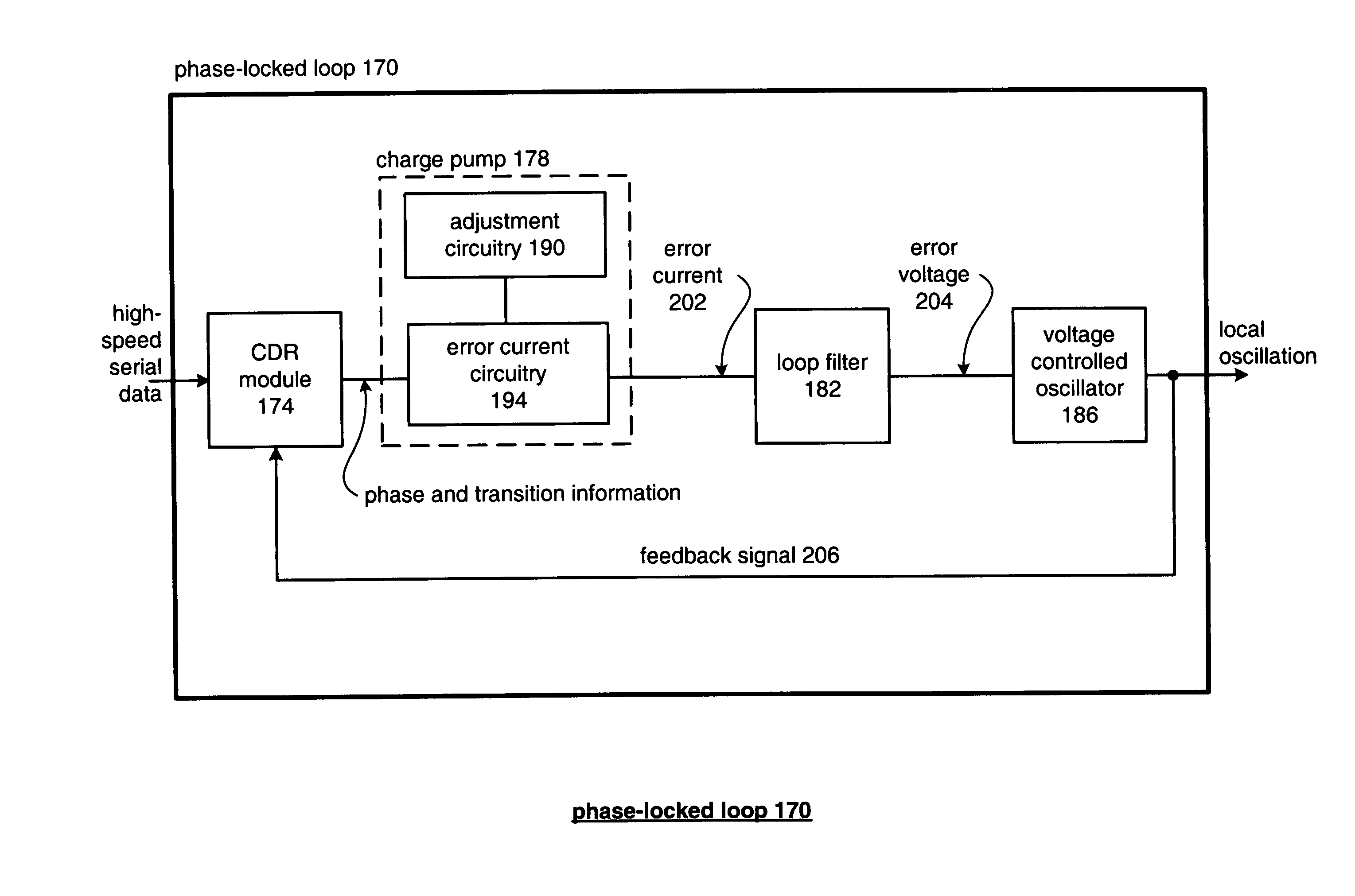
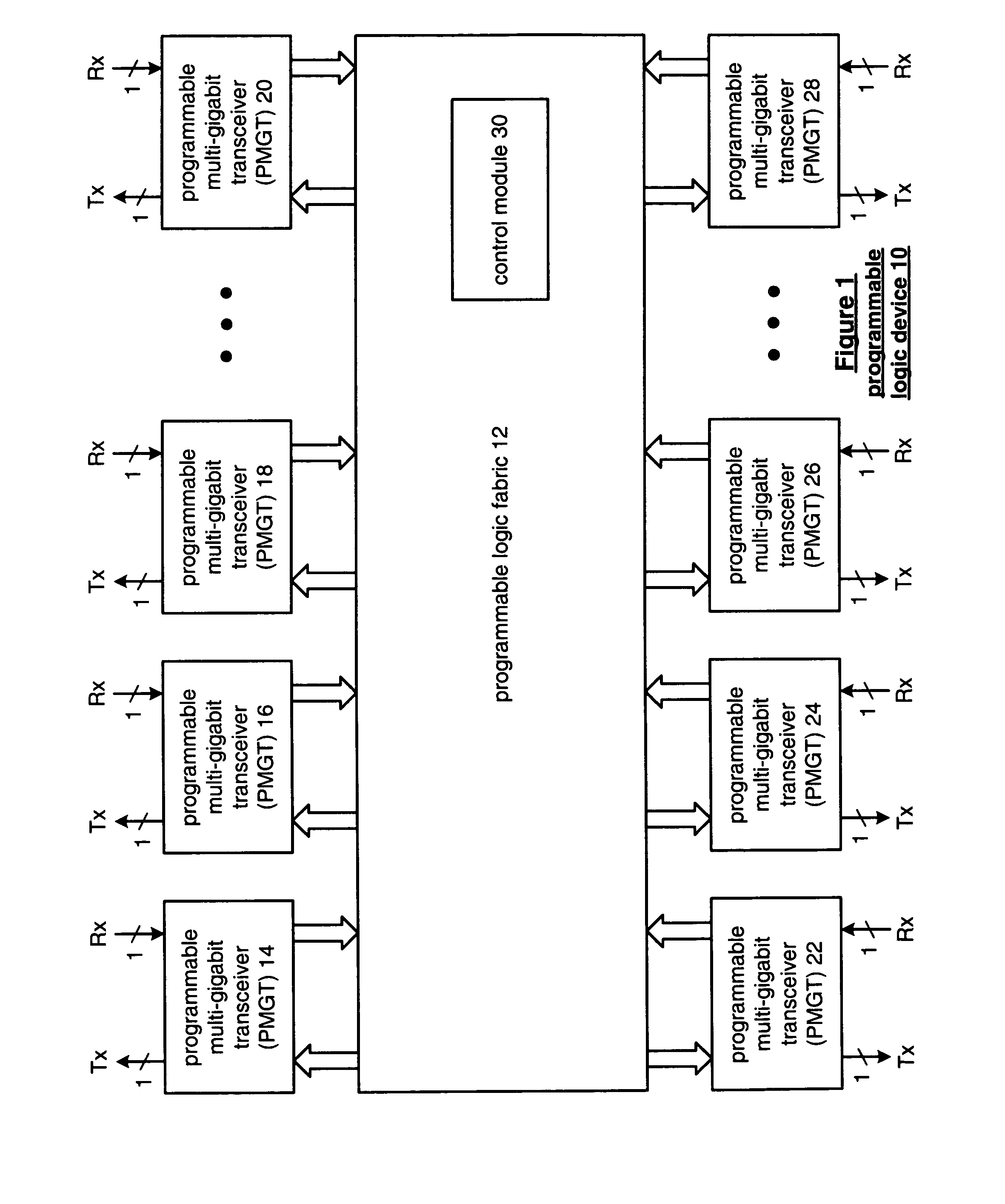
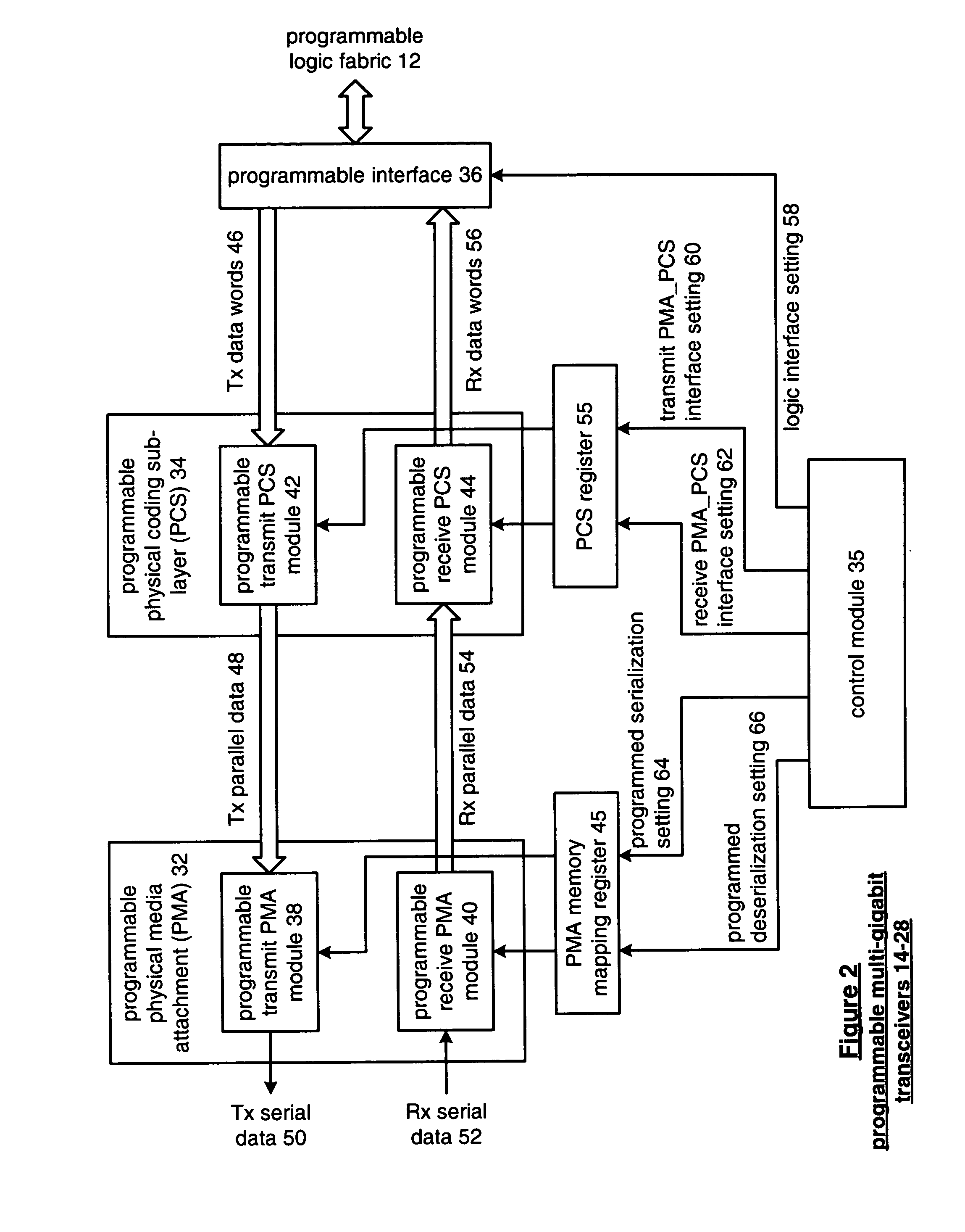
[0031]FIG. 1 is a schematic block diagram of a programmable logic device 10 that includes programmable logic fabric 12, a plurality of programmable multi-gigabit transceivers (PMGTs) 14–28 and a control module 30. The programmable logic device 10 may be programmable logic devices, an erasable programmable logic device, and / or a field programmable gate array (FPGA). When the programmable logic device 10 is an FPGA, the programmable logic fabric 12 may be implemented as a symmetric array configuration, a row-based configuration, a sea-of-gates configuration, and / or a hierarchical programmable logic device configuration. The programmable logic fabric 12 may further include at least one dedicated fixed processor, such as a microprocessor core, to further facilitate the programmable flexibility offered by programmable logic device 10.

[0032]The control module 30 may be contained within the programmable logic fabric 12 or it may be a separate module. In either implementation, the control m...


PUM


Abstract

Adjustment circuitry in a phase-locked loop (PLL) adjusts a sampling point to any desired location within a bit period of each bit of received high-speed serial data. The adjustment circuitry, responsive to program control, selectively adds current portions to a charge pump error current output thereby adjusting a feedback signal frequency to shift the serial data sampling point. A plurality of current mirror devices is scaled, with respect to a reference current device, to provide ΔI current portions. A current control module controls the current portions magnitude and a sign of the current portions. The adjustment circuitry further controls charge pump programmable current sources in order to set a desired operating point of the PLL. The programmable current sources are controlled by a bias voltage and a plurality of selectable serial and parallel coupled resistors.

Description

BACKGROUND OF THE INVENTION[0001]1. Technical Field of the Invention[0002]This invention relates generally to communication systems and more particularly to clock recovery circuits used therein.[0003]2. Description of Related Art[0004]Communication systems are known to transport large amounts of data between a plurality of end user devices, which, for example, include telephones, facsimile machines, computers, television sets, cellular telephones, personal digital assistants, etc. As is known, such communication systems may be local area networks (LANs) and / or wide area networks (WANs) that are stand-alone communication systems or interconnected to other LANs and / or WANs as part of a public switched telephone network (PSTN), packet switched data network (PSDN), integrated service digital network (ISDN), or the Internet. As is further known, communication systems include a plurality of system equipment to facilitate the transporting of data. Such system equipment includes, but is not...

Claims


Application Information

Patent Timeline
IPC IPC(8): H04B1/06
CPCH03L7/0896H03L7/0898H04L27/0014H04L2027/0067H04L2027/0055
Inventor BOECKER, CHARLES W.BRUNN, BRIAN T.
Owner XILINX INC
Features
  • Generate Ideas
  • Intellectual Property
  • Life Sciences
  • Materials
  • Tech Scout
  • Unparalleled Data Quality
  • Higher Quality Content
  • 60% Fewer Hallucinations
Learn More