Polymer based tunneling sensor

a technology of polymer and tunneling sensor, which is applied in the direction of speed/acceleration/shock measurement, measurement devices, instruments, etc., can solve the problem of only needing complex micro-machining steps, and achieve the effect of reducing noise tunneling sensor, eliminating noise components, and doubling the useful signal components

Inactive Publication Date: 2006-08-22
LOUISIANA TECH UNIV RES FOUND A DIV OF LOUISIANA TECH UNIV FOUND
View PDF15 Cites 13 Cited by
  • Summary
  • Abstract
  • Description
  • Claims
  • Application Information

AI Technical Summary

Benefits of technology

[0011]The invention further includes a reduced noise tunneling sensor. The reduced noise tunneling sensor has a first proof mass influencing a first tunneling tip. There is also a second proof mass having substantially the same mass as the first proof mass and also influencing a second tunneling tip. An indifference circuit is provided which receives a first signal related to movement of the first proof mass and a second signal related to movement of the second proof mass. The first and second signals have a useful signal component and a noise component and the indifference circuit subtracts the first and second signals, thereby doubling the useful signal component and eliminating the noise component.

Problems solved by technology

Moreover, for hot embossing of polymer materials, complex micro-machining steps are only necessary to fabricate a master mold.

Method used


Image

  • Polymer based tunneling sensor
  • Polymer based tunneling sensor
  • Polymer based tunneling sensor

Examples


example 1

[0033]This experiment involved the fabrication of silicon mold inserts by Inductive Coupled Etching (ICP). Current ICP processes can obtain aspect ratios of up to 40:1 and silicon molds have advantages (over conventional metal molds) such as fast and low-cost fabrication, flat surfaces, and suitable hardness, strength, and thermal conductivity. However, in practice ICP processes also have certain drawbacks which must be addressed. The two main drawbacks are area dependent etching (also called RIE lag) and micro-grass. This experiment presents an approach to overcome these two drawbacks through the fabrication of SOI (silicon on insulator) molds, and demonstrates the successful embossing of high-aspect-ratio micro-structures on PMMA.

[0034]“Area dependent etching” means that the etching depth is different for different open areas on a silicon wafer in the same process. In another words, the etching rate is faster for a wider trench than a narrower trench. The main reason is that the e...

example 2

[0040]The mold is formed from a silicon wafer subject to ICP dry etching in order to create the desired pattern. The pattern selected is a comb drive similar to that which created the structure seen in FIG. 3B. A high-aspect-ratio trench with a sidewall profile at 90° can be achieved with ICP. In order to remove the micro-grasses, the wafer was soaked in the standard KOH solution at 70° C. for several minutes.

[0041]The hot embossing system employed is the HEX 01 / LT, a commercial system from Jenoptik Mikrotechnik, located in Jena, Germany. The PMMA sheet is 0.5 mm thick with a glass transition temperature of 98° C. The entire fabrication procedures and parameters are the following: (1) open chamber and put PMMA on the substrate stage, (2) close chamber and evacuate it to 3 mTorr, (3) lower the mold to just touching the PMMA with a touch force of 300N, (4) heat mold and PMMA at the same time to 130° C. and keep this temperature for about 5 minutes, (5) insert the mold into PMMA under ...

example 3

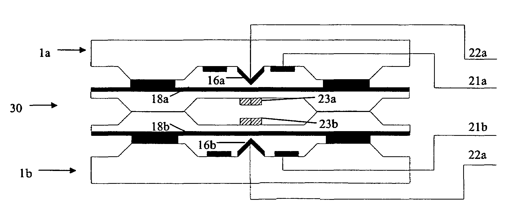
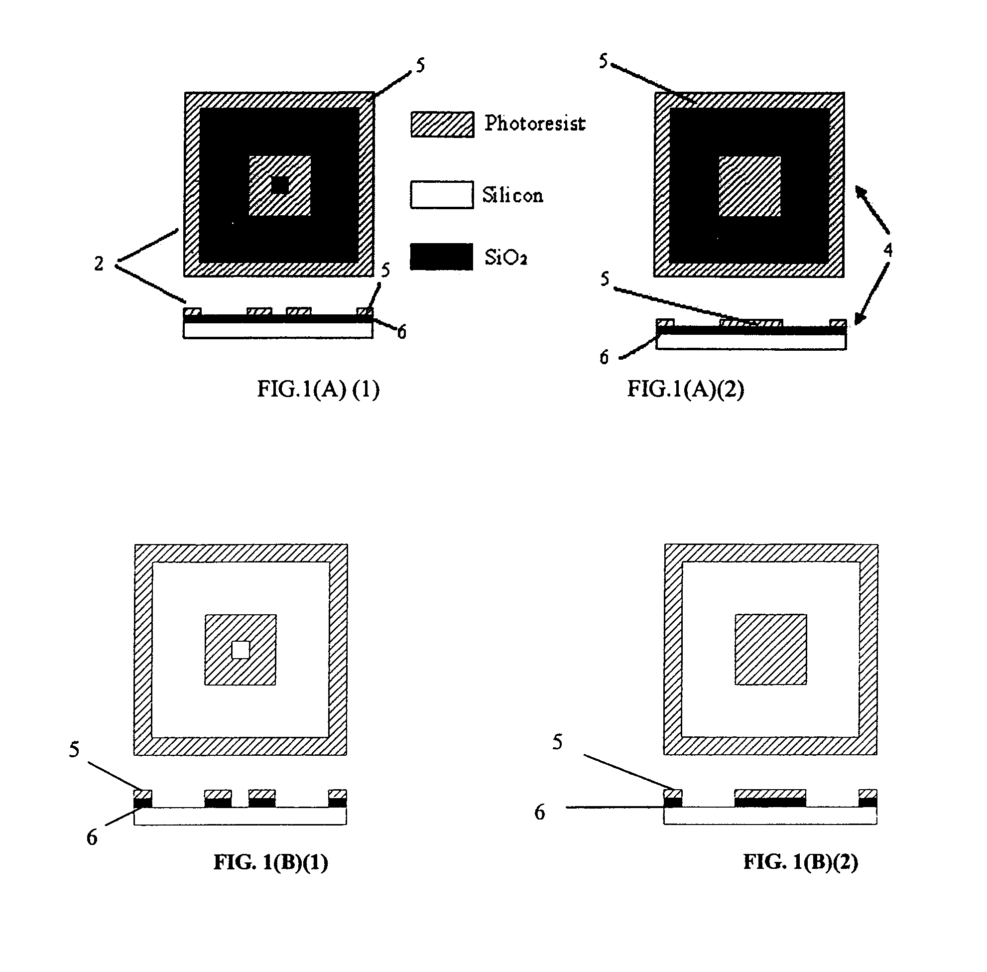
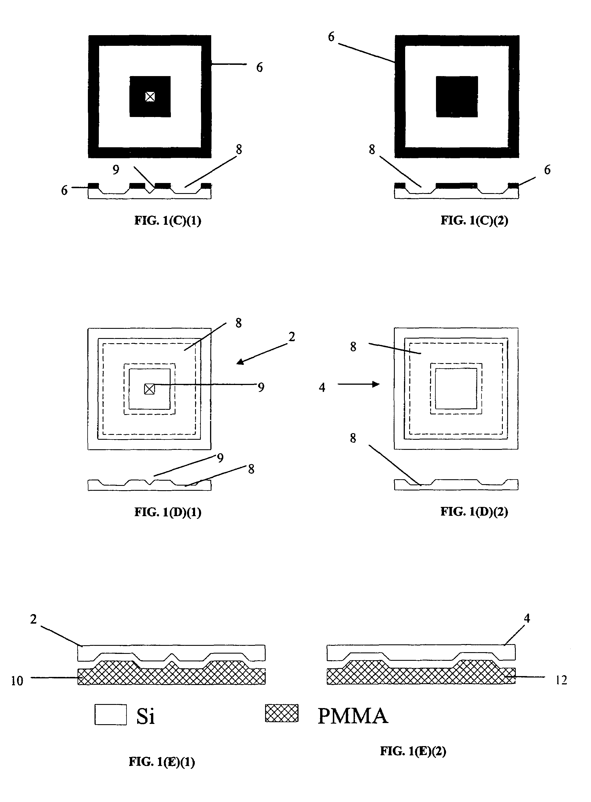
[0046]In order to manufacture the silicon molds, double-side polished silicon (100) wafers coated with 2 μm thermal oxide are selected. When using KOH wet etching, SiO2 layers are often used as the etching mask and since the etch ratio between SiO2 and Si is about 1 / 100. The thickness of SiO2 is chosen as 2 μm. In addition, the hot embossing process requires the molds to be bonded onto a holder, which requires the wafer have a smooth surface on its backside. The molds were designed to give a PMMA structure including a membrane of 30 μm in thickness and 2 mm×2 mm in square, a pyramid tunneling tip of 50 μm in height and 70 μm in base line, and a proof mass of 100 μm×100 μm in square and flexible in height. Small variations in the height are not generally critical since the sensors will be calibrated before use.

[0047]The preparation of silicon masters for hot embossing begins with KOH wet etching. Because KOH is a typical development liquid for positive photoresist, photoresist can no...


PUM

PropertyMeasurementUnit
feature sizesaaaaaaaaaa
shrinkageaaaaaaaaaa
thickaaaaaaaaaa

Abstract

A process for fabricating a polymer based circuit by the following steps. A mold of a design is formed through a lithography process. The design is transferred to a polymer substrate through a hot embossing process. A metal layer is then deposited over at least part of said design and at least one electrical lead is connected to said metal layer.

Description

STATEMENT REGARDING FEDERALLY SPONSORED RESEARCH OR DEVELOPMENT[0001]This work was supported at least in part by the U.S. Government under grants: NSF / LEQSF (2001-04)-RII-02, DARPA DAAD19-02-1-0338, and NASA (2002)-Stennis-22. The U.S. government has certain rights in this invention.CROSS-REFERENCE TO RELATED APPLICATION[0002]None.FIELD OF INVENTION[0003]The present invention relates to electronic circuits formed from polymer materials. In particular, the present invention relates to circuits formed by a hot embossing process and tunneling sensor circuits.BACKGROUND OF INVENTION[0004]Polymer materials have been of great interest in the research and development of integrated circuits (IC) and micro-electro-mechanical systems (MEMS) recently due to their relatively low cost and much simpler processing techniques. Hot embossing of polymers is a promising alternative to the traditional silicon processes. It fulfills the demand for low-cost methods of mass production of micro-components ...

Claims


Application Information

Patent Timeline
Patent Type & Authority Patents(United States)
IPC IPC(8): H01L21/00
CPCB81C99/0085G01P15/0894G01P15/0802B81B2201/0292B81C2203/038
Inventor CUI, TIANHONGWANG, JINGZHAO, YONGJUN
Owner LOUISIANA TECH UNIV RES FOUND A DIV OF LOUISIANA TECH UNIV FOUND
Why Eureka
Try Eureka