Electronic device, method of manufacture of the same, and sputtering target

a technology of electronic devices and sputtering targets, applied in the field of electronic devices, can solve the problems of increasing the contact resistance between the signal conductor and the pixel electrode, deteriorating display quality of the screen, and difficulty in neglecting the increase in manufacturing costs and the accompanying productivity decline, so as to reduce manufacturing man-hour and cost, reduce manufacturing costs, and eliminate barriers. metal

Inactive Publication Date: 2006-08-29
KOBE STEEL LTD
View PDF21 Cites 67 Cited by
  • Summary
  • Abstract
  • Description
  • Claims
  • Application Information

AI Technical Summary

Benefits of technology

[0012]This invention is devised paying attention to the situation as described above. It is the object thereof to establish a technology that enable elimination of a barrier metal as described above and simplification of the process without increasing the number of steps, and can make an aluminum alloy film contact with the electrode directly and surely. Another object is to make excellent electric properties capable of realizing low electrical resistivity and low contact resistance compatible with heat resistance, and to establish a technology that enables commonality of material between the reflective electrode and a TAB connection electrode in the display device.
[0021]In putting this method in practice, a precipitate (an intermetallic compound) can be formed in the contact interface between the aluminum alloy film and the first electrode by making a part or all of the alloy components forming a solid solution in a non-equilibrium state as the aluminum alloy film and alloy components of the first electrode diffuse mutually. Moreover, as a preferable method of forming the aluminum alloy film, the sputtering method is exemplified. Furthermore, it is preferable that an insulating film is formed on the aluminum alloy film to make a lamination, contact hole etching is performed on the insulating film, and successively after this the aluminum alloy wiring is subjected to light etching by 1 to 200 nm, more preferably 3 to 100 nm, from the aluminum alloy surface, and thereby a precipitate (intermetallic compound) of a part or all of alloy components forming a solid solution in a non-equilibrium state is exposed partly. This is because contact resistance between itself and the first electrode formed thereon can be further reduced.
[0024]The invention constructed as described above makes it possible to directly contact between the aluminum alloy film and the electrode, alleviate the manufacturing man-hour and cost by eliminating the barrier metal. And thereby the invention can provide the electronic device and the array substrate having the properties of low-cost and high-performance.
[0025]According to the present invention, any one of noble metals hard to oxidize, such as Au and Ag, or elements each of whose oxide has a comparatively low electrical conductivity, such as Zn, Co, Ni, Sr, Ge, and Sm, or an element that has a low solid solubility limit in aluminum, such as Bi, in trace amounts is made to be contained in an aluminum alloy film. And an area having a low electric resistance is formed partly or all-over in the contact interface between the first electrode and the second electrode (aluminum alloy film) without deteriorating electrical conductivity of the film itself as a wiring material. Consequently the contact resistance between the first electrode and the second electrode (aluminum alloy film) is reduced considerably, making possible to reduce the number of steps and manufacturing cost considerably. Furthermore, when this invention is applied to the liquid crystal display, the display quality thereof can be maintained at a high level. Furthermore, heat resistance can be increased considerably by adding at least one element selected from Nd, Y, Fe, and Co.

Problems solved by technology

Then, if an insulating material layer is formed in the contact interface between the signal conductors and the pixel electrode in this way, the contact resistance between the signal conductors and the pixel electrode will increase and the display quality of a screen will deteriorate.
However, as the cost of a liquid crystal panel etc. keeps to be reduced by mass production, it has become difficult to neglect the increase in the manufacturing cost and the decrease in productivity accompanying the formation of a barrier metal.
On the other hand, according to U.S. Pat. No. 6,252,247, deposition of the gate electrode, the source electrode, or the drain electrode can be performed continuously in the same deposition chamber, but increase in the number of steps cannot be avoided.
Besides, when the chamber is used continuously, there occurs frequently a phenomenon that films peel off the wall of the chamber due to a difference of thermal expansion coefficient between a film into which impurities have been mixed and a film into which no impurity has been mixed, and consequently the equipment must be halted frequently because of maintenance.
Moreover, according to the patent document 1, indium tin oxide (ITO) that is most popular at present must be altered to indium zinc oxide (IZO), which increases material cost.

Method used


Image

  • Electronic device, method of manufacture of the same, and sputtering target
  • Electronic device, method of manufacture of the same, and sputtering target
  • Electronic device, method of manufacture of the same, and sputtering target

Examples


embodiments

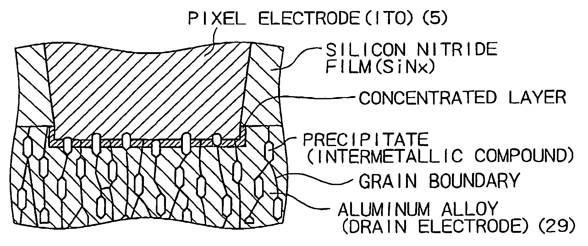
[0129]Next, Table 1 shows measurement results of the contact resistance between the pixel electrodes 5 and the aluminum alloy film when the aluminum alloy film directly contacts the pixel electrode 5 on the array substrate according to this invention.

[0130]The measurement experiment was conducted as follows.

[0131]1) Composition of pixel electrode: indium tin oxide (ITO) with 10 wt % tin oxide added to indium oxide, or indium zinc oxide (IZO) with 10 wt % zinc oxide added to indium oxide. Each film thickness is 200 nm.

[0132]2) Composition of aluminum wiring film: alloy component contents are as shown in Table 1.

[0133]3) Heat treatment conditions: After depositing an insulating film (SiNx) with a thickness of 300 nm, it is processed by heat treatment in a vacuum at 300° C. for 1 hour.

[0134]4) Light etching: The insulating film (SiNx) is dry-etched using fluorine system plasma, and successively after this each aluminum wiring material is etched by approximately 10 nm and further etched...


PUM

PropertyMeasurementUnit
thicknessaaaaaaaaaa
diameteraaaaaaaaaa
diameteraaaaaaaaaa

Abstract

In an electronic device comprising a first electrodes consisting of a metal oxide and a second electrode consisting of an aluminum alloy film directly contacted and electrically connected to the first electrode, the contact interface between the aluminum alloy film and the first electrode is constructed so that at least a part of alloy components constituting the aluminum alloy film exist as a precipitate or concentrated layer. This construction enables direct contact between the aluminum alloy film and the electrode consisting of a metallic oxide and allows elimination of a barrier metal in such an electronic device, and manufacturing technology therefor.

Description

BACKGROUND OF THE INVENTION[0001]1. Field of the Invention[0002]This invention relates to an electronic device in a thin film form, the method of its manufacture, and a sputtering target. Specifically the invention relates to a novel display device comprising, as its constituents, pixel electrodes used in active and passive matrix type flat panel displays such as semiconductor displays and liquid crystal displays, reflective films, optical components etc., and aluminum alloy film; the method of its manufacture; and the sputtering target.[0003]2. Description of the Related Art[0004]For example, the active matrix type liquid crystal display uses thin film transistors (TFT) as switching elements, and is composed of a TFT array substrate equipped with a wiring section of pixel electrodes, scan lines, signal conductors, etc., an opposed substrate equipped with a common electrode that is disposed in opposition to the TFT array substrate with a predetermined spacing, and a liquid crystal l...

Claims


Application Information

Patent Timeline
Patent Type & Authority Patents(United States)
IPC IPC(8): H01L23/52H01L23/48G02F1/1343C23C14/18C23C14/34G02F1/1335H01L21/28H01L21/285H01L21/3205H01L21/336H01L21/768H01L21/77H01L21/84H01L27/12H01L27/13H01L29/45H01L29/49H01L29/786
CPCC23C14/185C23C14/3414G02F1/133553H01L29/458H01L29/4908H01L29/66757H01L29/66765H01L27/124H01L27/1255Y10T428/12H01L2924/0002H01L2924/00H01L29/786
Inventor GOTOH, HIROSHIKUGIMIYA, TOSHIHIRONAKAI, JUNICHITOMIHISA, KATSUFUMI
Owner KOBE STEEL LTD
Why Eureka
Try Eureka