Nitride semiconductor device comprising bonded substrate and fabrication method of the same

a technology of nitride and semiconductor devices, which is applied in the direction of semiconductor devices, superconductor devices, electrical devices, etc., can solve the problems of low device structure, low thermal conductivity, and limited device size, so as to reduce the size of the device and reduce the structure of the devi

Inactive Publication Date: 2006-09-12
NICHIA CORP
View PDF67 Cites 79 Cited by
  • Summary
  • Abstract
  • Description
  • Claims
  • Application Information

AI Technical Summary

Benefits of technology

[0006]However, sapphire is an insulator with a low thermal conductivity and it limits the structure of a device. For example, in the case of a conductor substrate of such as GaAs and GaP, electric contact parts (electrode), one on the top face of a semiconductor apparatus and another in the bottom face, can be formed, whereas in the case of a light emitting device grown on sapphire, two electric contact parts should be formed on a top face (on a single face). Therefore, if an insulating substrate of such as sapphire is used, the effective light emitting surface area for the same substrate surface area is narrowed as compared with that of a conductor substrate. Further, in the case of using an insulating substrate, the number of devices (chips) that can be obtained from a wafer with the same Φ is low.

Problems solved by technology

However, sapphire is an insulator with a low thermal conductivity and it limits the structure of a device.
Further, in the case of using an insulating substrate, the number of devices (chips) that can be obtained from a wafer with the same Φ is low.
Also, since wires are required respectively for both p and n electrodes in wire bonding process for the electrodes, the chip size becomes large to result in decrease of yield of the chips.
However, in the case a nitride semiconductor device is grown on a SiC substrate, no electrode can be directly formed in the side of the nitride semiconductor layer where the layer contacts with the SiC substrate.
However, the conductivity and the thermal conductivity of SiC are not sufficient.

Method used


Image

  • Nitride semiconductor device comprising bonded substrate and fabrication method of the same
  • Nitride semiconductor device comprising bonded substrate and fabrication method of the same
  • Nitride semiconductor device comprising bonded substrate and fabrication method of the same

Examples


example 1

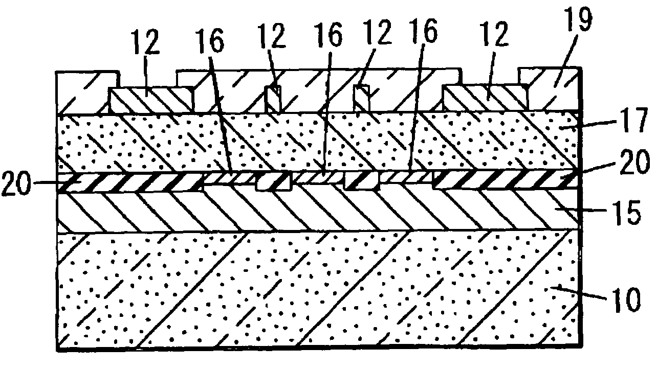
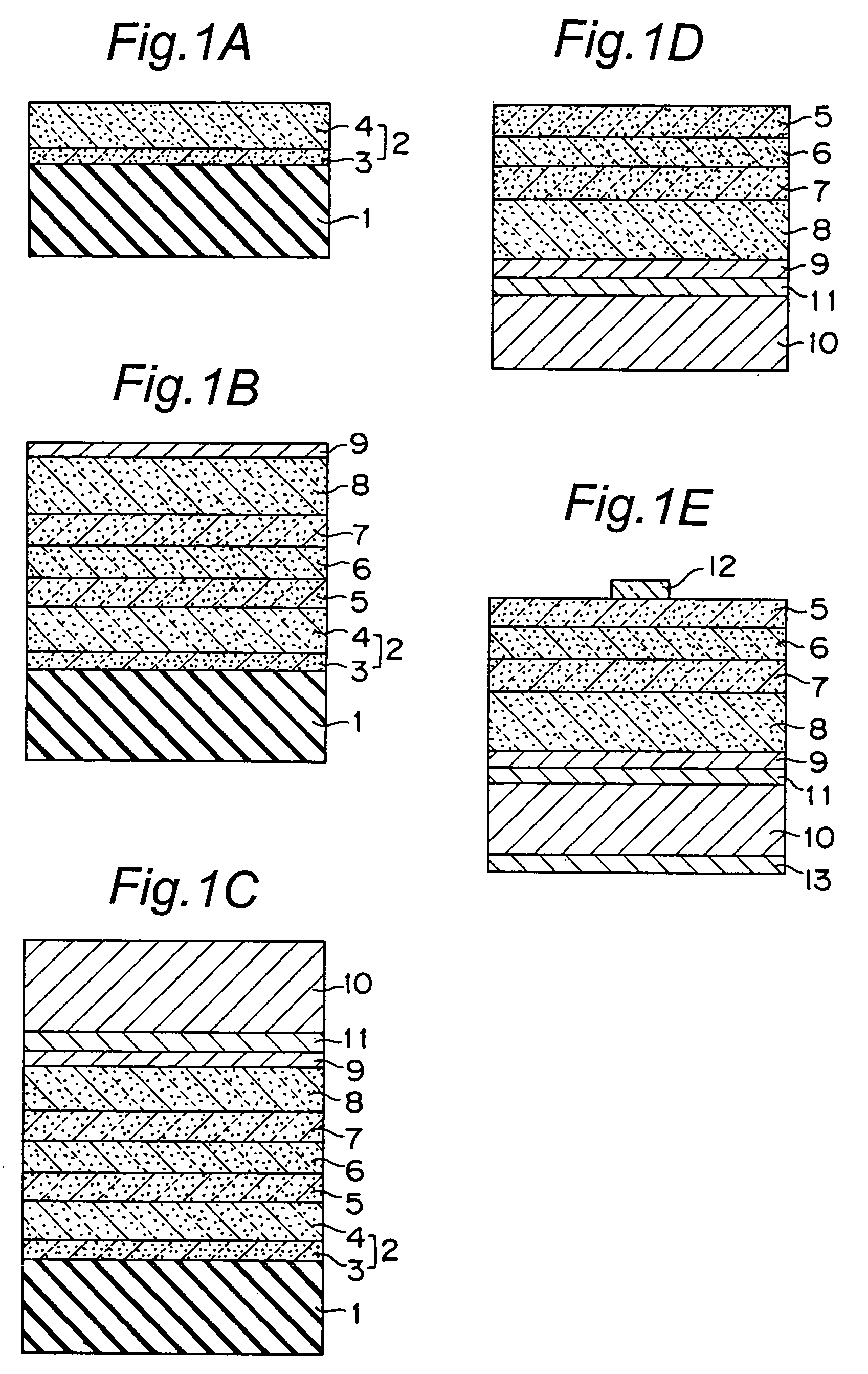
[0169]In this Example, the invention was applied to a light emitting diode with 375 nm wavelength and a nitride semiconductor device was produced according to a fabrication method of the invention as illustrated in FIGS. 1A to 1E.

(Substrate for Growing Nitride Semiconductor)

[0170]A substrate of sapphire (C-plane) was used as a substrate for growing nitride semiconductor 1 and surface cleaning was carried out at 1,050° C. in hydrogen atmosphere in a MOCVD reaction vessel.

(Under Layer 2)

[0171]Buffer layer 3: Successively, a buffer layer 3 of GaN in a thickness of about 200 Å was grown on the substrate at 510° C. in hydrogen atmosphere using ammonia and TMG (trimethylgallium).

(High Temperature Grown Layer 4)

[0172]High temperature grown layer 4: After growth of the buffer layer 3, a high temperature grown nitride semiconductor 4 of undoped GaN in 5 μm thickness was grown on the substrate by stopping only TMG supply, increasing the temperature to 1,050° C., and using TMG and ammonia as r...

example 2

[0185]An LED obtained in the same manner under same conditions as those of Example 1 except that the p-type electrode in the first bonding layer with a thickness of 2,000 Å was formed using Ag had output power of 5.8 mW and Vf of 4.2V.

example 3

[0186]This Example was carried out under same conditions as those of Example 1 except that the laser radiation method was employed in place of the polishing method at the time of removing the substrate for growing nitride semiconductor 1.

(Removal of Substrate for Growing Nitride Semiconductor 1)

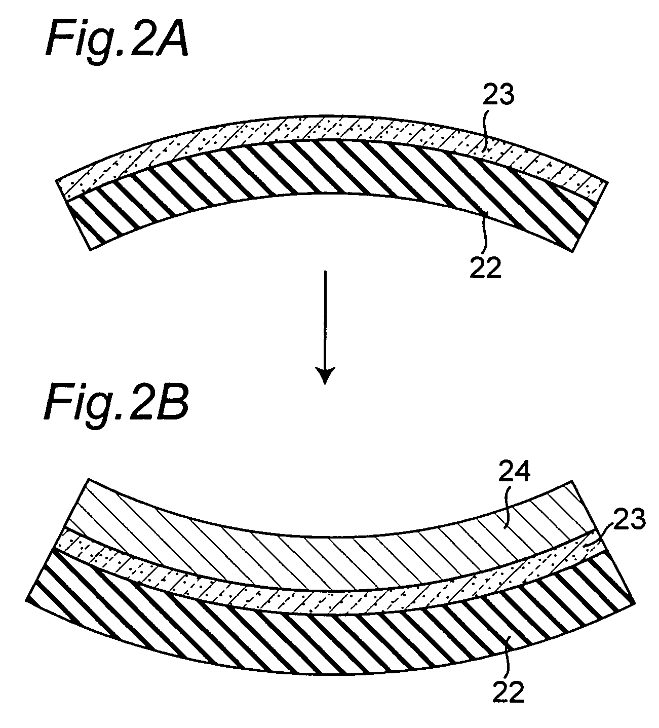
[0187]With respect to the laminate for bonding to which the conductive supporting substrate 10 was bound, laser beam in linear state of 1 mm×50 mm was radiated with an output power of 600 J / cm2 to the entire surface of the opposed face of the sapphire substrate 1 from the under layer side by scanning using KrF excimer laser with wavelength of 248 nm. The nitride semiconductor of the under layer 2 was decomposed by the laser radiation to remove the sapphire substrate 1.

[0188]The obtained LED had luminescence peak wavelength of 373 nm at 20 mA electric power in forward direction and had Vf of 3.47 V and output power of 4.2 mW. Further, as compared with the case of Example 1, since the sapphire ...


PUM

PropertyMeasurementUnit
luminescent wavelengthaaaaaaaaaa
thicknessaaaaaaaaaa
thicknessaaaaaaaaaa

Abstract

A substrate 1 for growing nitride semiconductor has a first and second face and has a thermal expansion coefficient that is larger than that of the nitride semiconductor. At least n-type nitride semiconductor layers 3 to 5, an active layer 6 and p-type nitride semiconductor layers 7 to 8 are laminated to form a stack of nitride semiconductor on the first face of the substrate 1. A first bonding layer including more than one metal layer is formed on the p-type nitride semiconductor layer 8. A supporting substrate having a first and second face has a thermal expansion coefficient that is larger than that of the nitride semiconductor and is equal or smaller than that of the substrate 1 for growing nitride semiconductor. A second bonding layer including more than one metal layer is formed on the first face of the supporting substrate. The first bonding layer 9 and the second bonding layer 11 are faced with each other and, then, pressed with heat to bond together. After that, the substrate 1 for growing nitride semiconductor is removed from the stack of nitride semiconductor so that a nitride semiconductor device is provided.

Description

BACKGROUND OF THE INVENTION[0001]1. Field of the Invention[0002]The invention relates to a fabrication method of a nitride semiconductor device comprising a nitride semiconductor (InxAlyGa1-x-yN, 0≦x, 0≦y, x+y≦1), such as a light emitting diode (LED), a laser diode (LD); light receiving devices such as a solar cell, a photosensor; or electronic devices such as a transistor, a power device; and the like.[0003]2. Description of the Related Art[0004]Owing to the stability in the high temperature ammonia atmosphere in its epitaxial growth process, it has been proved that sapphire is a desirable substrate for growing a light emitting device of a high efficiency made of nitride semiconductor. Practically, a nitride semiconductor device grown on a sapphire substrate is employed for a high brightness blue emitting LED, a pure green LED, and LD (laser diode) and it is applied for full color displays, signal display apparatus, image scanners, light sources such as a light source for optical d...

Claims


Application Information

Patent Timeline
Patent Type & Authority Patents(United States)
IPC IPC(8): H01L31/12H01L21/762H01L33/06H01L33/12H01L33/32H01L33/44H01L33/50
CPCH01L21/76251H01L33/0079H01L33/32H01L33/44H01L2224/49171H01L2224/48247H01L2224/48091H01L2924/3025H01L2224/45144H01L2924/01037H01L33/483H01L33/508H01L33/62H01L2924/01013H01L2924/00014H01L2924/00H01L33/0093H01L2924/12032
Inventor NAGAHAMA, SHINICHISANO, MASAHIKOYANAMOTO, TOMOYASAKAMOTO, KEIJIYAMAMOTO, MASASHIMORITA, DAISUKE
Owner NICHIA CORP
Why Eureka
Try Eureka