Process for adjusting data structures of a floorplan upon changes occurring

a technology of floorplan and data structure, applied in the field of floorplan data structure adjustment upon changes occurring, can solve the problems of increasing complexity of integrated circuits in general, affecting the performance of workstations, and unable to so as to improve performance and meet timing and power consumption constraints.

Active Publication Date: 2006-10-10
XILINX INC
View PDF11 Cites 38 Cited by
  • Summary
  • Abstract
  • Description
  • Claims
  • Application Information

AI Technical Summary

Benefits of technology

[0023]The teachings of the invention contemplate data structures, computer processes, programmed computers and computer readable media which contain instructions to control a computer to provide a new floor planning tool. These inventions implement a floor planning tool which allows users to creates new physical hierarchies to place circuits (instances) from a logical netlist (which contains no physical placement information) onto a floorplan of any integrated circuit and allows any instance from the logical netlist to be put into any physical block of a floorplan. This allows the user to give guidance to a place and route tool on where specific circuits are to be placed in the final chip layout so as to enhance performance and ensure that timing and power consumptions constraints can be met. This floor planning tool is useful in laying out conventional integrated circuits, FPGAs, ASICS, structured ASICs and any other type of integrated circuit.
[0024]The physical blocks define a physical hierarchy, and the computer processes allow invasion of the logical blocks of the netlist to get information needed to define the instances that have been assigned to various pblocks. Extensive use of pointers in the data structures of the physical hierarchy are used to save storage space needed to store the data structures of the physical hierarchy. These pointers point to data in data structures of the logical hierarchy so that this data does not have to be repeated in the data structures of the physical hierarchy.
[0027]Each pblock has its own data object which defines the location of the pblock on the floor plan of the integrated circuit (chip) being designed. The floorplan provides the proposed placement of the circuits to be integrated on said chip. Each pblock data object also includes a list of child pblocks, said child pblocks being pblocks which are contained within the parent pblock. Each pblock data object includes a list of instances or circuits that are assigned to the pblock. Each instance entry on the list is implemented through use of a pointer to the data object which defines the instance in the original logical netlist thereby reducing the amount of data that needs to be stored for the physical hierarchy.
[0029]Use of pblocks and a physical hierarchy to define the positions of circuits on chip floorplans greatly improves the performance of the chip because the logical netlist includes no position information. This leaves it up to the place and route tool to put circuits on the chip surface wherever it determines they need to be. This can result in some circuits being placed too far away from each other to meet timing constraints or power consumption constraints. By allowing the designer to place pblocks on a chip floorplan and then populate them with circuits from the logical netlist, a designer can place circuits that have hard to meet timing and power constraints close to each other in the final design. This decreases the amount of parasitic capacitance (parasitic capacitance is proportional to length) in the conductive lines between the chips and reduces the propagation delays and power consumption on these shorter lines.
[0060]6) Another subspecies is to make each pblock stand alone in the sense that all nets into or out of the pblock terminate on a pblock boundary pin, and each pblock has its own timing and power constraints for its nets. In this way, large netlists do not have to be stored in their entirety in the RAM of the place and route workstation. Instead, individual pblocks can be output from the floor planning tool to the place and route tool as if each individual pblock was its own stand alone chip. This allows place and route tools to work with large netlists using the directives output by the floor planner tool without exceeding the RAM capacity of the machine.

Problems solved by technology

However, increasingly complex integrated circuits in general are increasing in popularity because integration of large systems on a chip substantially reduces manufacturing costs over other classic forms of construction of circuits.
In complex integrated circuits, the netlist can be so large that it cannot all be stored in the RAM available on the workstation.
This results in part of the netlist being stored on the hard disk of the workstation and being paged in and out of RAM.
This slows down the workstation and can be frustrating for the designer.
Long lines of conductive material running across the chip between terminals of devices that need to communicate signals cause excessive amounts of parasitic capacitance.
Parasitic capacitance slows down the operation of integrated circuits and limits the upper frequency of the clock speed that controls all switching on the chip.
This makes this space less useable because it is more difficult to integrate other circuitry in this space and get connections to it without interference with the other lines running across the space.
This was not optimal because it might result in placement of circuits that need to communicate with each other which are in different logical blocks far from each other on the chip.
Still, any data at all for the physical hierarchy in addition to the large logical netlist aggravates the memory shortage problem for the place and route tool on complex designs.
Large netlists and large physical directives files complicates and slows down the operations of all both the floor planner tool and the place and route tool if the size of the netlist and physical directive file exceeds the available RAM capacity.
Frequently, place and route tools cannot handle all the gates in a large netlist even if they have 4 gigabytes of RAM.
If the place and route tool or the floor planner tool cannot have all of the netlist in RAM, it will not operate unless virtual memory is turned on and part of the netlist on the workstation hard disk.
Putting part of the netlist on hard disk and paging it in and out of RAM has not proved to be a desirable solution as it is very slow.
Big logical netlists and compact representations of a physical layout still create problems for place and route tools though because this data can still exceed the capacity of the RAM of the workstation upon which the place and route tool is executing.
In other words, while the place and route tool is thinking, it generates large amounts of trial and error placement and routing data on proposed placements that must be stored.
However, if the place and route tool runs out of RAM during this process, complications will arise.
Place and route tools are not very deterministic though.
Prior art floor planner tools were restricted to working with the logical blocks defined in the logical netlist.
If one floor plans with only the logical blocks defined by the netlist, it is often not possible to get the best performance.
Performance issues would require that these two different circuits be placed close to each other on the chip.
But if the floor planner is restricted to placement of logical blocks, it is possible that the two circuits in different logical blocks that need to communicate will not be placed close enough together on the chip to achieve optimum performance.
This aggravates the memory shortage problem

Method used


Image

  • Process for adjusting data structures of a floorplan upon changes occurring
  • Process for adjusting data structures of a floorplan upon changes occurring
  • Process for adjusting data structures of a floorplan upon changes occurring

Examples


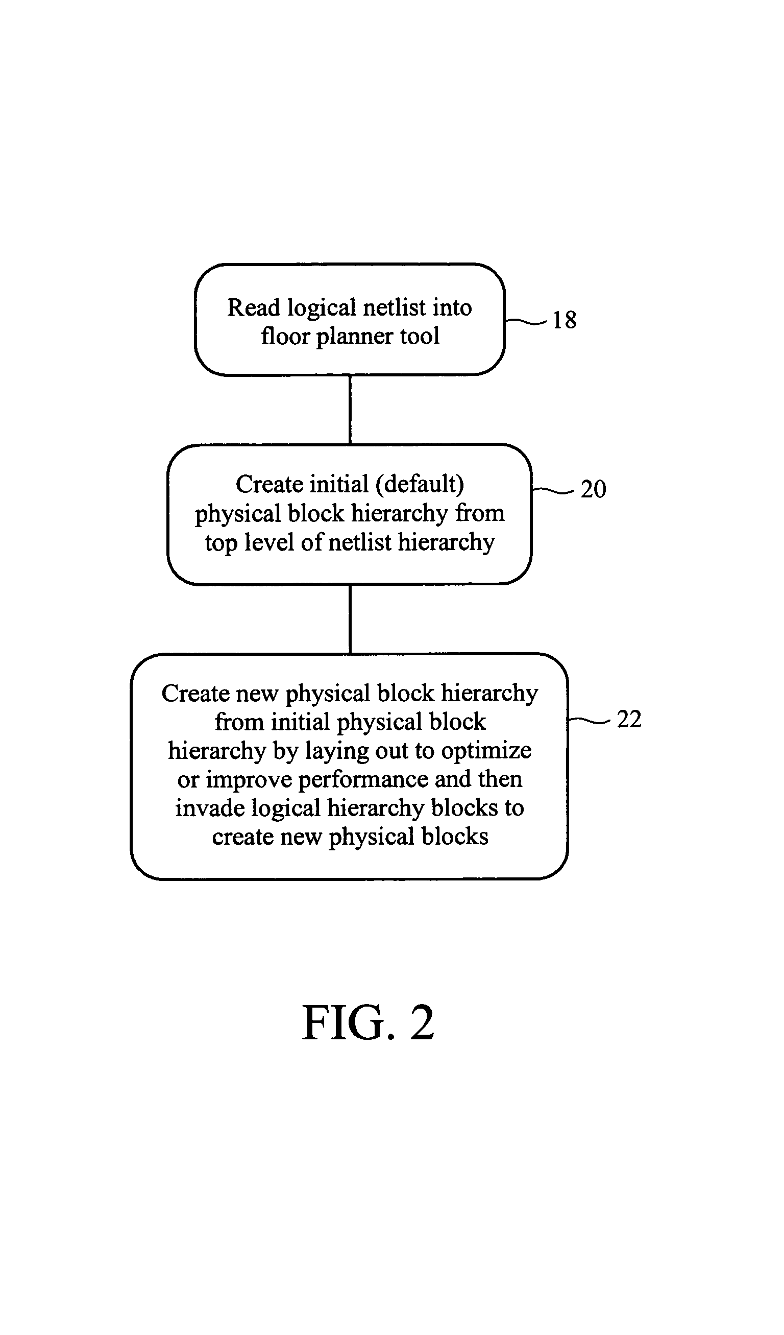
Embodiment Construction

[0078]Definitions

[0079]The teachings of the invention contemplate a general purpose computer coupled to a display, a keyboard and a pointing device and programmed with an operating system which executes as an application the floor planning software to be described below. The computer typically has a hard disk, and one or more ports for inputting and outputting data and may have a CD-ROM drive, floppy disk drive, DVD-RAM drive etc. to read in data stored on portable media.

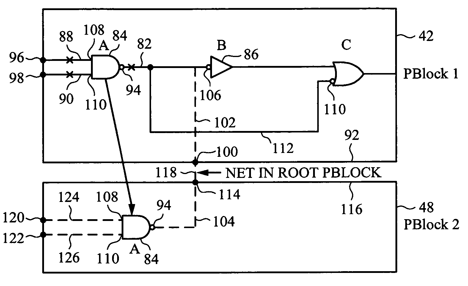
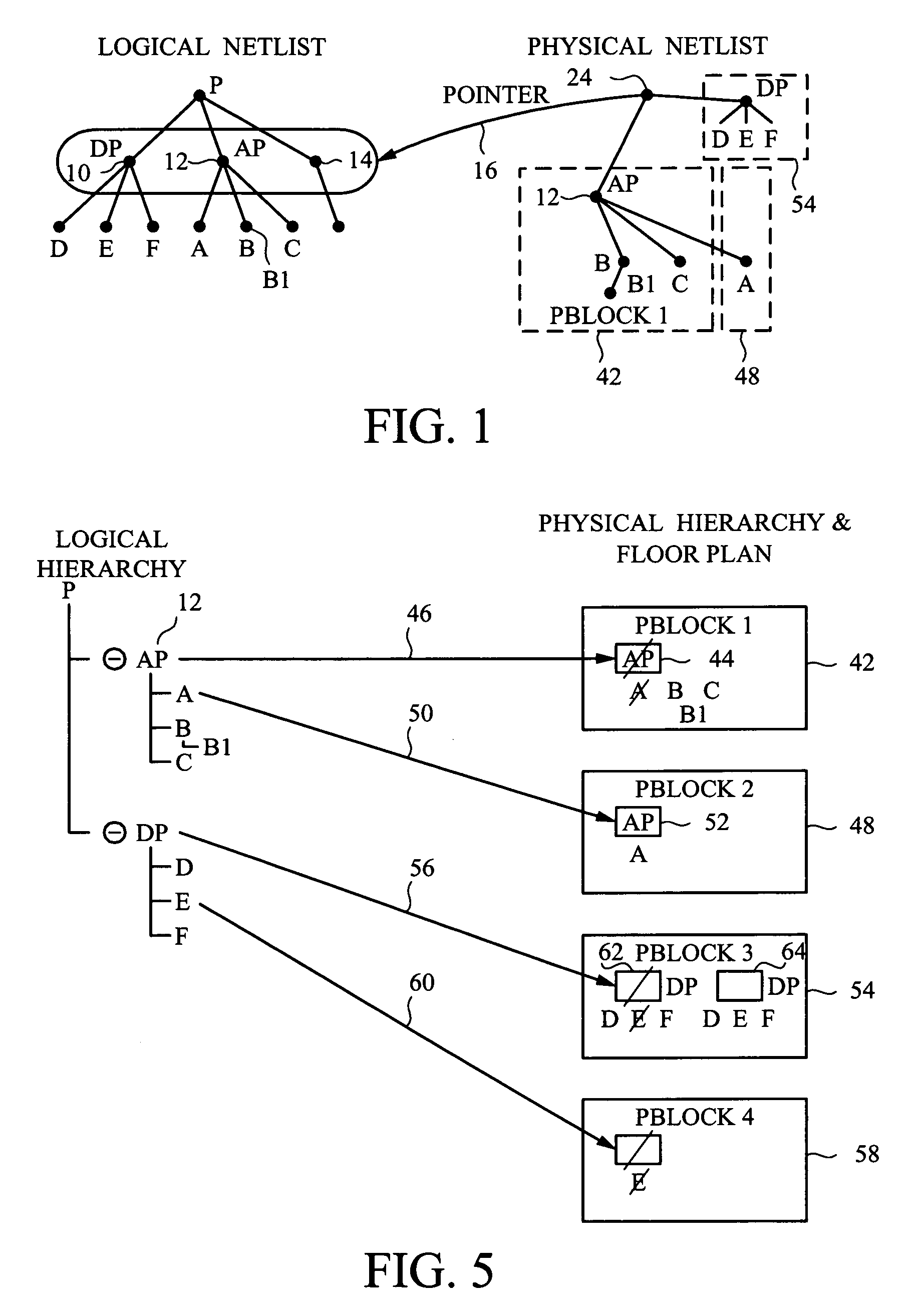
[0080]To best understand the descriptions herein, consider the following terminology definitions.[0081]Instance—a piece or block of logic. It can be ‘flat’ (aka primitive), e.g., something simple and indivisible like an ‘AND’ or ‘NOT’. It can also be hierarchical—e.g., something that is defined by and includes at a lower level in a hierarchy, individual instance of simpler circuits such as a set of flat instances to form a more complex block of logic, such as an ALU or large RAM.[0082]Pin—represents an input or outp...


PUM


Abstract

A floor planner tool for integrated circuit design which provides tools and displays for a designer to create a floor plan to define desired placement of circuits defined in a logical netlist by creating a physical hierarchy comprised of nested pblocks. Each pblock is a data structure which contains data which defines which circuits from the logical netlist are assigned to it. Each pblock stands alone and can be input to a place and route tool without the rest of the physical hierarchy. Each pblock data structure contains pointers to the circuits on the netlist assigned to that plbock, identifies other pblocks nested within it and contains at least a list of boundary pins for that pblock.

Description

[0001]This patent is a co-pending application of U.S. patent application entitled “System for Representing the Logical and Physical Information of an Integrated Circuit”, by David A. Knol and Salil Ravindra Raje, filed on Mar. 3, 2004, Ser. No. 10 / 792,164, of which is herein incorporated by reference.FIELD OF USE AND BACKGROUND OF THE INVENTION[0002]Field programmable gate arrays (FPGAs) and application specific integrated circuits are increasingly popular types of integrated circuits. However, increasingly complex integrated circuits in general are increasing in popularity because integration of large systems on a chip substantially reduces manufacturing costs over other classic forms of construction of circuits.[0003]When designing integrated circuits, the final design is reduced to a file called a netlist. A netlist is a description of the devices that are to be fabricated on an integrated circuit and the connections between each terminal of each device to form the circuit.[0004]...

Claims


Application Information

Patent Timeline
Patent Type & Authority Patents(United States)
IPC IPC(8): G06F17/50G06F9/45
CPCG06F17/5072G06F30/392
Inventor KNOL, DAVID A.RAJE, SALIL RAVINDRA
Owner XILINX INC
Why Eureka
Try Eureka