Dielectric anti-reflective coating surface treatment to prevent defect generation in associated wet clean

Inactive Publication Date: 2006-10-24
INTEGRATED DEVICE TECH INC
View PDF18 Cites 14 Cited by
  • Summary
  • Abstract
  • Description
  • Claims
  • Application Information

AI Technical Summary

Benefits of technology

[0007]Accordingly, the present invention provides a method for preventing the formation of watermark defects, particularly before the formation of shallow trench isolation structures. In one embodiment, a method for preventing the formation of watermark defects includes the steps of sequentially forming a pad oxide layer, a silicon nitride layer and a silicon oxynitride layer over a semiconductor substrate. A photore

Problems solved by technology

One problem encountered with the use of silicon oxynitride is that this material is not compatible with hydrogen fluoride (HF) or buffered oxide etch (BOE) based wet clean processes.
Moreover, the surface of plasma-based silicon oxynitride is very hydrophilic.
These characteristics result in the formation of small amounts of water containing micro bumps (i.e., watermarks) on a silicon oxynitride layer when the silicon oxynitride is present during an HF or ROE based wet clean process.
These watermarks are difficult to remove.
The presence of watermarks can result in defects that are hereinafter referred to as watermark defects.
A waterm

Method used


Image

  • Dielectric anti-reflective coating surface treatment to prevent defect generation in associated wet clean
  • Dielectric anti-reflective coating surface treatment to prevent defect generation in associated wet clean
  • Dielectric anti-reflective coating surface treatment to prevent defect generation in associated wet clean

Examples


Example

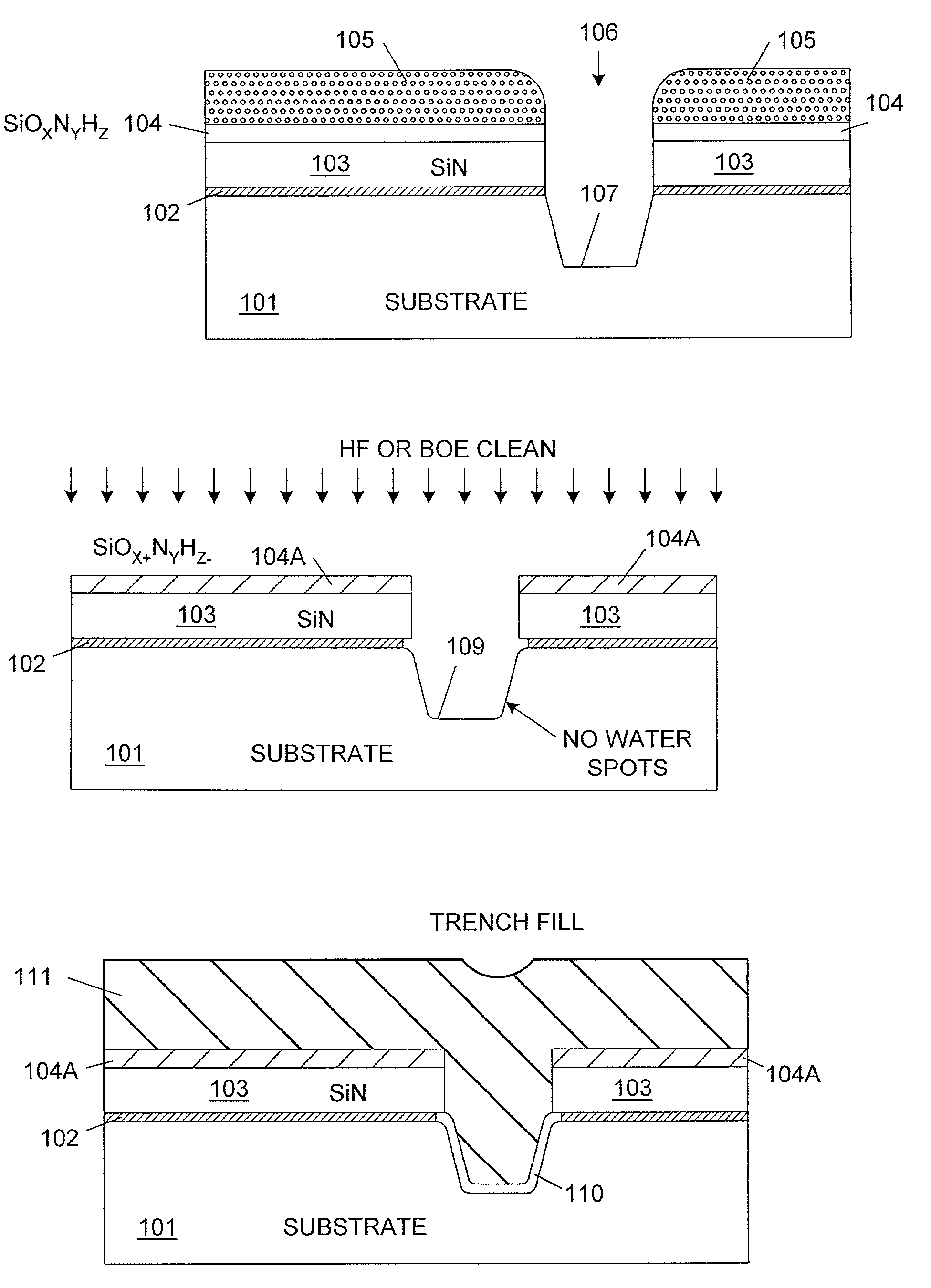
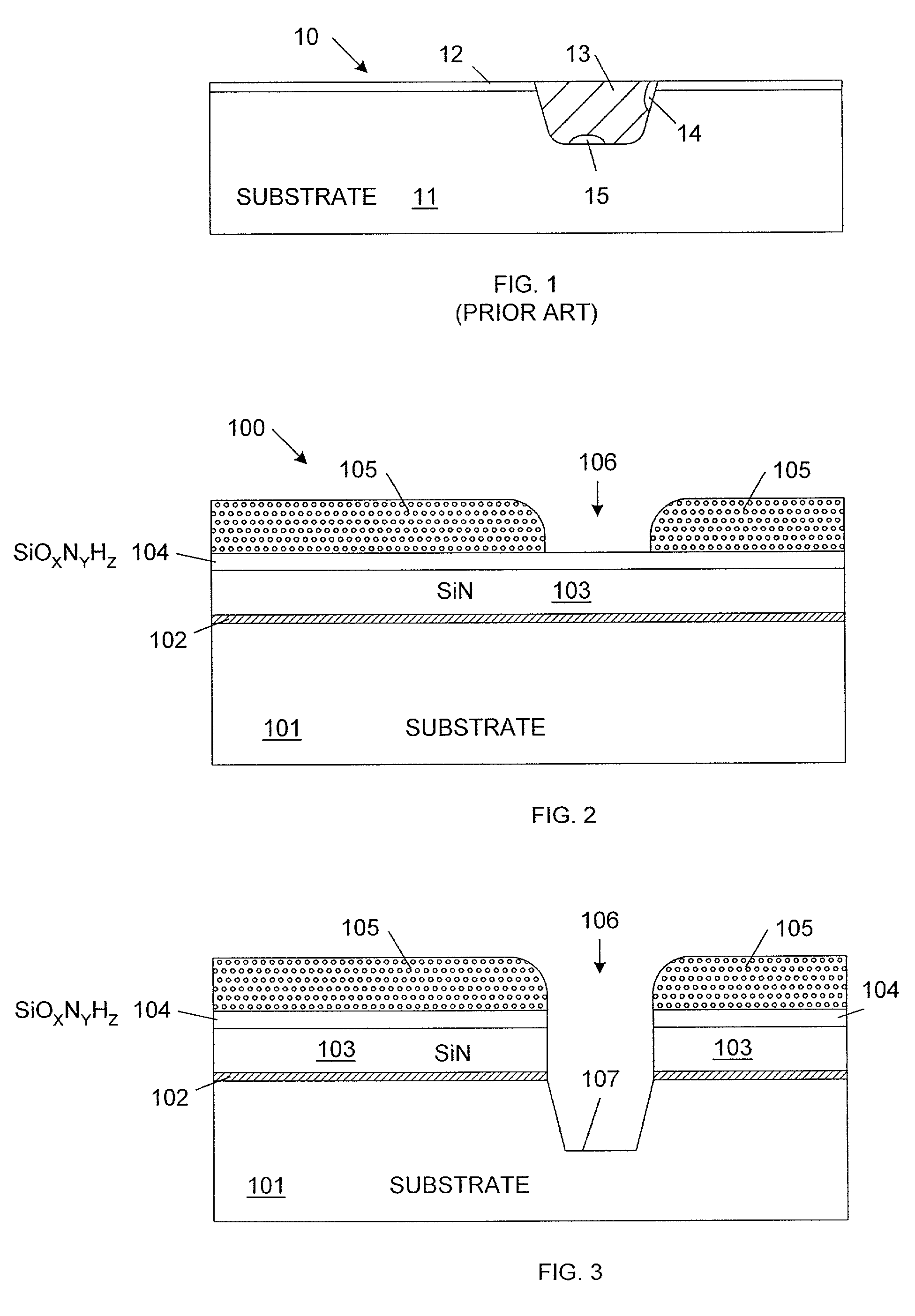
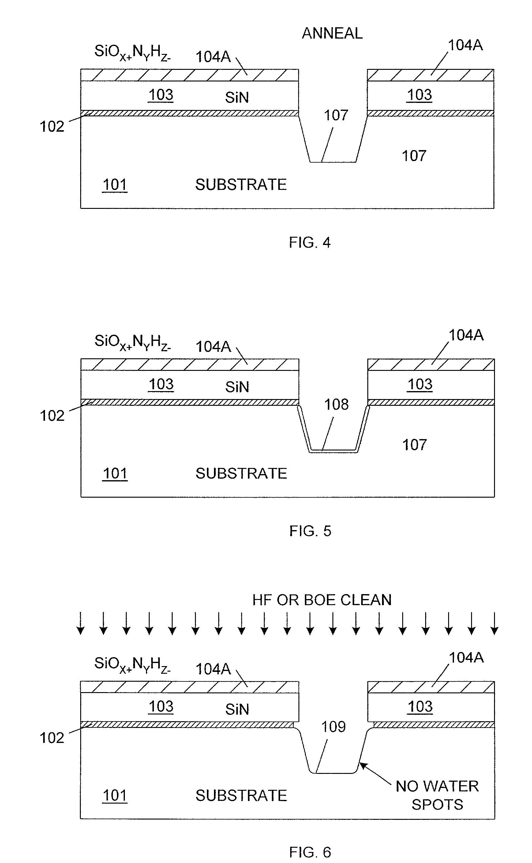
[0015]FIGS. 2–9 are cross-sectional diagrams of a semiconductor process for preventing the formation of watermark defects in accordance with one embodiment of the present invention.

[0016]As illustrated in FIG. 2, semiconductor structure 100 includes semiconductor substrate 101, pad oxide 102, silicon nitride layer 103, silicon oxynitride layer 104 and photoresist mask 105. In the described embodiment, semiconductor substrate 101 is a lightly doped monocrystalline silicon substrate having a crystal structure of . However, other semiconductor substrates can be used in other embodiments of the invention.

[0017]In the described embodiment, pad oxide 102 is a layer of silicon oxide that is thermally grown at the upper surface of substrate 101 to a thickness in the range of about 80 to 150 Angstroms. Pad oxide 102 is grown using processing techniques that are well known to those of ordinary skill in the art.

[0018]Silicon nitride (SiN) layer 103 is then deposited over pad oxide 102 to a thi...


PUM


Abstract

A method for preventing the formation of watermark defects includes the steps of forming a pad oxide, a silicon nitride layer and a silicon oxynitride layer over a semiconductor substrate. A photoresist mask is formed over the resulting structure, with the silicon oxynitride layer being used as an anti-reflective coating during exposure of the photoresist material. An etch is performed through the photoresist mask, thereby forming a trench in the substrate. The photoresist mask is stripped, and the silicon oxynitride layer is conditioned. For example, the silicon oxynitride layer may be conditioned by a rapid thermal anneal in the presence of oxygen or nitrogen. A wet clean step is subsequently performed to remove a native oxide layer in the trench. The conditioned silicon oxynitride layer prevents the formation of watermarks during the wet clean process.

Description

FIELD OF THE INVENTION[0001]The present invention relates to the prevention of defects during a semiconductor process. More specifically, the present invention relates to a method for preventing watermark defects when an anti-reflective coating (ARC) is used in conjunction with a wet clean.RELATED ART[0002]Plasma-deposited silicon oxynitride (SiXOYNZHA), is a dielectric material that has been used as an anti-reflective coating (ARC) on critical layers in photolithographic processes. One problem encountered with the use of silicon oxynitride is that this material is not compatible with hydrogen fluoride (HF) or buffered oxide etch (BOE) based wet clean processes. Plasma-based silicon oxynitride is a complex material having an unusually rich hydrogen (H) content of about 15% and poor film density. Moreover, the surface of plasma-based silicon oxynitride is very hydrophilic. These characteristics result in the formation of small amounts of water containing micro bumps (i.e., watermarks...

Claims


Application Information

Patent Timeline
IPC IPC(8): H01L21/762H01L21/027H01L21/306H01L21/311H01L21/314H01L21/768
CPCH01L21/0276H01L21/31111H01L21/3143H01L21/76235H01L21/76814H01L21/76829H01L21/02052Y10S438/906Y10S438/952H01L21/022
Inventor LO, GUO-QIANGPAN, OHM-GUOYU, ZHENJIANGMAO, YU-LUNGSYAU, TSENGYOULEE, SHIH-KED
Owner INTEGRATED DEVICE TECH INC
Why Eureka
Try Eureka