Reducing defect formation within an etched semiconductor topography

a technology of etched semiconductors and defect formation, applied in the direction of semiconductor/solid-state device manufacturing, basic electric elements, electric devices, etc., can solve the problems of preventing sufficient contact, increasing the resistance of contact, failure of a subsequently formed integrated circuit, etc., to reduce the formation of defects or remove them

Inactive Publication Date: 2006-10-31
MONTEREY RES LLC
View PDF17 Cites 19 Cited by
  • Summary
  • Abstract
  • Description
  • Claims
  • Application Information

AI Technical Summary

Benefits of technology

[0008]The problems outlined above may be in large part addressed by a method for processing a semiconductor topography. In particular, a method is provided which includes etching one or more layers in an etch chamber while introducing a noble gas heavier than helium into the etch chamber. In a preferred embodiment, the introduction of such a noble gas may reduce the formation of or remove defects within an etched portion of the semiconductor topography. Such defects may include, for example, bilayer mounds comprising nitride and a material comprising silicon. In some cases, the defect...

Problems solved by technology

Depending on a defect's size, location, and composition, a defect within a device may cause a failure within a subsequently formed integrated circuit.
For example, a defect in a contact may increase resistance of the contact or may even prevent sufficient contact to the underlying structure.
In other cases, defects may cause elevational disparities within a semiconductor topography, thereby making further deposition of layers and fabrication of structures difficult.
Failures within integrat...

Method used


Image

  • Reducing defect formation within an etched semiconductor topography
  • Reducing defect formation within an etched semiconductor topography
  • Reducing defect formation within an etched semiconductor topography

Examples


Embodiment Construction

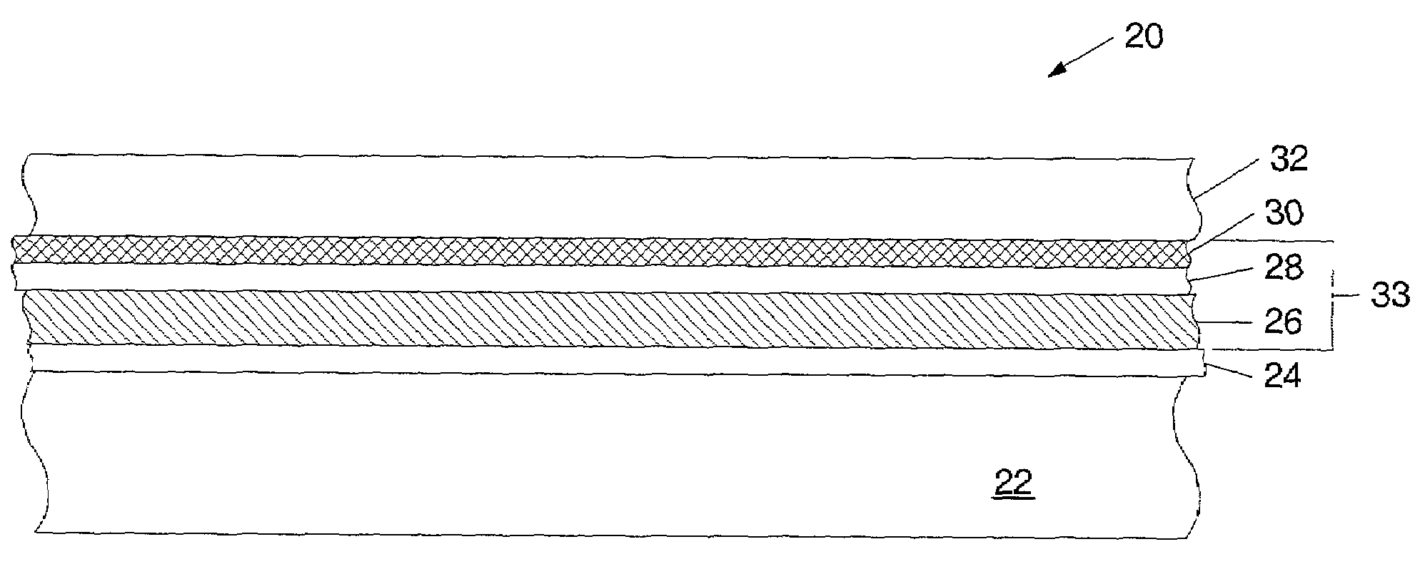
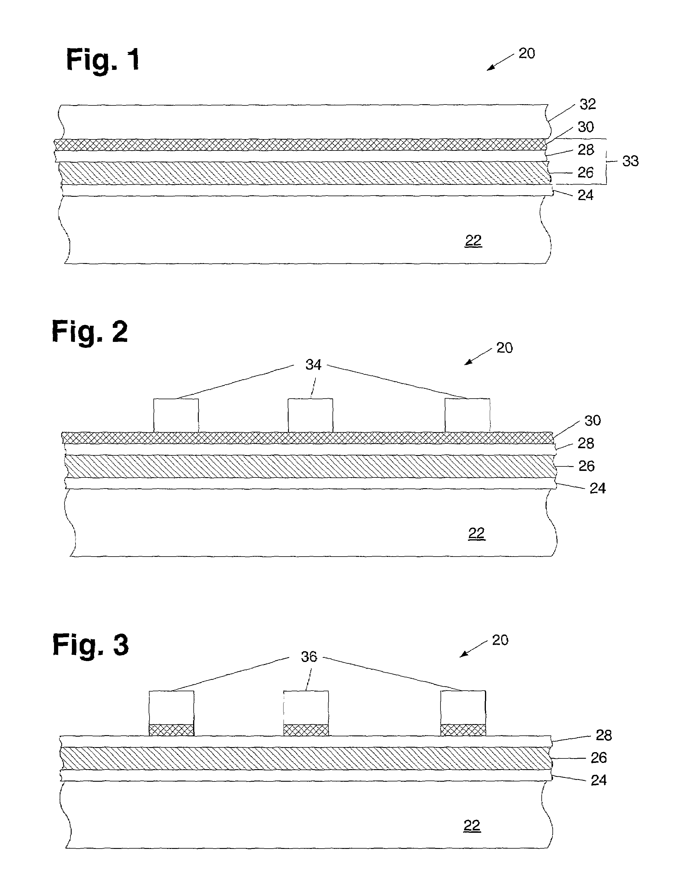
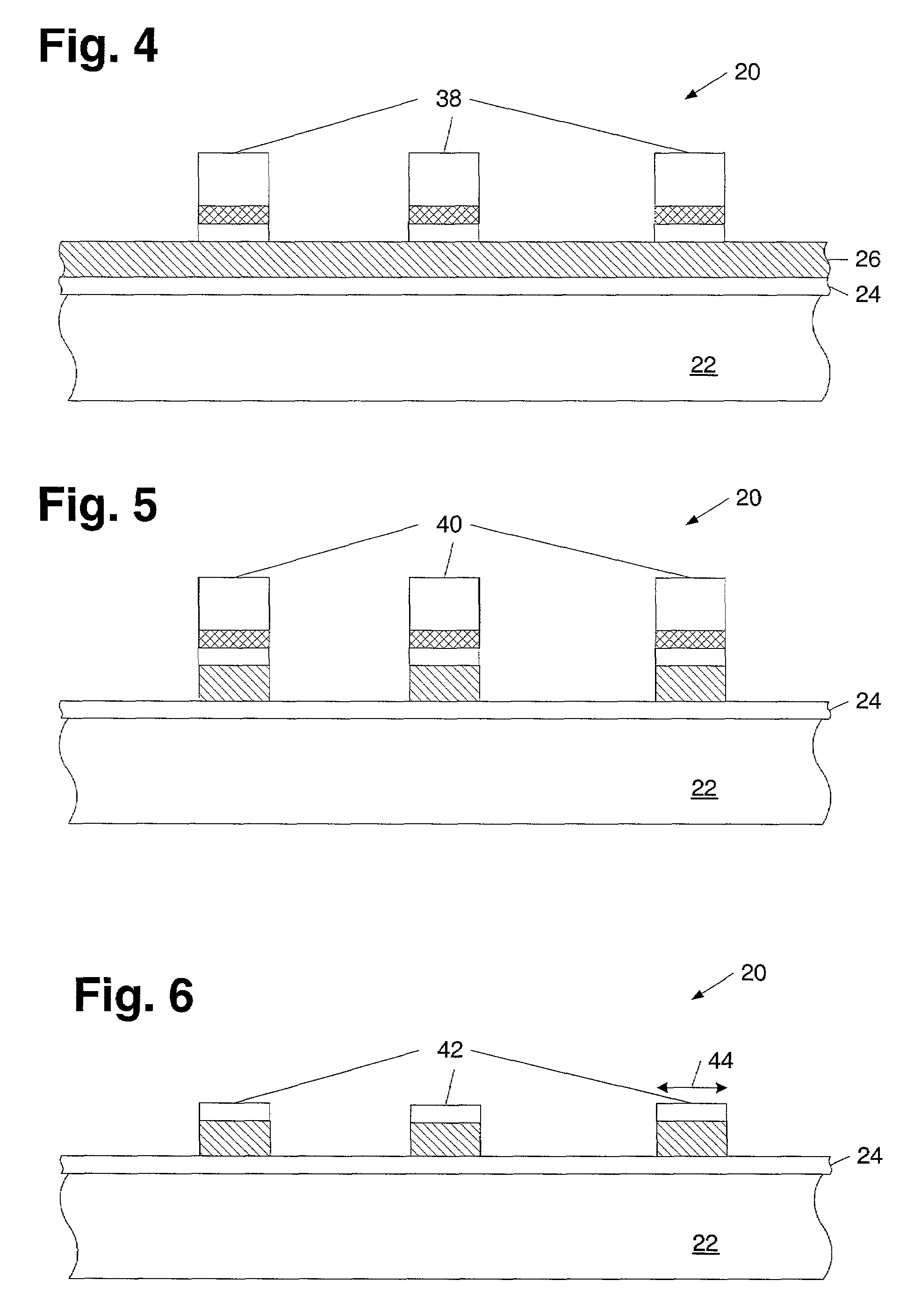
[0028]Turning to the drawings, exemplary embodiments of a method for processing a semiconductor topography are shown in FIGS. 1–12. In particular, a method is provided which includes etching one or more layers in an etch chamber while introducing a noble gas heavier than helium into the etch chamber. In a preferred embodiment, the introduction of such a noble gas may reduce the formation of or remove defects within an etched portion of the semiconductor topography. FIG. 1 depicts a partial cross-sectional view of semiconductor topography 20 in which a plurality of layers is formed upon and in contact with each other. In particular, semiconductor topography 20 may include dielectric 24 interposed between semiconductor layer 22 and stack of layers 33. In some cases, dielectric 24 may be regarded as part of stack of layers 33. Alternatively, dielectric 24 may be considered separate from stack of layers 33. In addition, resist layer 32 may be formed above stack of layers 33. In some emb...


PUM


Abstract

A method is provided which includes etching one or more layers in an etch chamber while introducing a noble gas heavier than helium into the etch chamber. In a preferred embodiment, the introduction of such a noble gas may reduce the formation of defects within an etched portion of the semiconductor topography. Such defects may include bilayer mounds of nitride and a material comprising silicon, for example. In some embodiments, the method may include etching a stack of layers within a single etch chamber. The stack of layers may include, for example, a nitride layer interposed between an anti-reflective layer and an underlying layer. In addition, the single etch chamber may be a plasma etch chamber designed to etch materials comprising silicon. As such, the method may include etching an anti-reflective layer in a plasma etch chamber designed to etch materials comprising silicon.

Description

BACKGROUND OF THE INVENTION[0001]1. Field of the Invention[0002]This invention relates to semiconductor device manufacturing, and more particularly, to an improved method for processing a semiconductor topography.[0003]2. Description of the Related Art[0004]The following descriptions and examples are not admitted to be prior art by virtue of their inclusion within this section.[0005]In general, it is desirable to have an integrated circuit fabrication process produce a semiconductor device with structures and spaces within certain dimension specifications. In some cases, the dimensions of structures and spaces within a device may be referred to as critical dimensions. “Critical dimension” (CD), as used in this application, may generally refer to the dimensional design value of a feature. Critical dimensions are of interest since they may represent the smallest dimension that may be formed on a semiconductor topography using various techniques such as photolithography and etch proces...

Claims


Application Information

Patent Timeline
IPC IPC(8): H01L21/302H01L21/461
CPCH01L21/31116H01L21/31138H01L21/32136H01L21/32137
Inventor SCHWARZ, BENJAMIN C. E.YAN, CHAN LONBAMNOLKER, HANNAARNZEN, DANIEL J.
Owner MONTEREY RES LLC
Why Eureka
Try Eureka