
Micro electro-mechanical system device with piezoelectric thin film actuator

a micro electromechanical system and actuator technology, applied in generators/motors, variable capacitors, instruments, etc., can solve the problems of inconvenient tunable limited operation of electrostatic rf mems switch, and inability to adapt to commercial handheld products, etc., to achieve low operating voltage, improve performance characteristics, and less stiction problems

Inactive Publication Date: 2006-11-07
RAYTHEON CO
View PDF9 Cites 26 Cited by
  • Summary
  • Abstract
  • Description
  • Claims
  • Application Information

AI Technical Summary

Benefits of technology

The present invention provides an RF MEMS device with a piezoelectric thin film actuator that has improved performance characteristics such as low operating voltage, variable RF tuning capacity, fewer stiction problems, simplified fabrication, and improved switching time. The RF MEMS device can be used in low signal loss switches, phase shifters, filters, and receivers for radar and communication products, as well as wireless infrastructure and consumer products. The piezoelectric thin film actuator has a movable end that can be controlled to vary the interelectrode spacing between the RF path electrode and the conducting path electrode, resulting in a variable capacitance that can be selectedively controlled. The piezoelectric thin film actuator includes a piezoelectric layer that expands or contracts longitudinally when a voltage potential is applied, and an elastic layer that converts the longitudinal expansion or contraction of the piezoelectric layer into transverse movement of the cantilever end of the piezoelectric actuator. The conducting path electrode is transverse the longitudinal extent of the piezoelectric thin film actuator and has a width at least as long as the gap between the RF-in and RF-out path electrodes. The RF circuit substrate may include a GaAs layer. The method for manufacturing the RF MEMS device includes steps of providing an RF circuit substrate with an RF conducting path, fabricating a piezoelectric thin film actuator, and assembling the actuator to the RF circuit substrate. The piezoelectric thin film actuator has improved performance characteristics such as low operating voltage, variable RF tuning capacity, fewer stiction problems, simplified fabrication, and improved switching time.

Problems solved by technology

Consequently, the switch is not suitable for applications such as commercial handheld products, which typically operate on 3 volts or less.
The electrostatic RF MEMS switch also is limited in its operation, as it can only be open or closed, that is, either in contact or not in contact.
For this reason, the electrostatic RF MEMS switch is not suitable as a tunable capacitor, as such devices typically require controlled variance in the displacement of the actuation beam.
Electrostatic RF MEMS switches also suffer from a well known problem known as stiction, which occurs when surface tension forces are higher than the spring restoring force of the actuator beam.
Stiction may be caused by a wet etching process used during fabrication, which may leave some moisture or meniscus which pulls the beam towards the electrode and prevents the beam from releasing.
Stiction is a major problem of electrostatic RF MEMS switches, oftentimes rendering the switch inoperable.
Since the silicon has a low resistivity which may interfere with the RF performance of the circuit, typically a switch manufacturer removes the silicon, leaving only the actuator on the RF circuit.
For high volume applications, this additional silicon removal step may be quite costly.
Electrothermal actuated devices also are not without drawbacks.
The electrothermal actuator has some limitations such as slower tuning and more space requirements.
Controllably cooling down the beam is difficult, as the amount of time to sufficiently cool the beam oftentimes is not ascertainable or is met with inconsistent results.
Although the actuator may be made smaller to reduce its cooling time, the cooling time still cannot be controlled effectively to vary the interelectrode spacing and hence the capacitance between the electrodes.

Method used


Image

  • Micro electro-mechanical system device with piezoelectric thin film actuator
  • Micro electro-mechanical system device with piezoelectric thin film actuator
  • Micro electro-mechanical system device with piezoelectric thin film actuator

Examples


Embodiment Construction

[0045]In the detailed description which follows, identical components have been given the same reference numerals, regardless of whether they are shown in different embodiments of the present invention. To illustrate the present invention in a clear and concise manner, the drawings may not necessarily be to scale and certain features may be shown in somewhat schematic form.

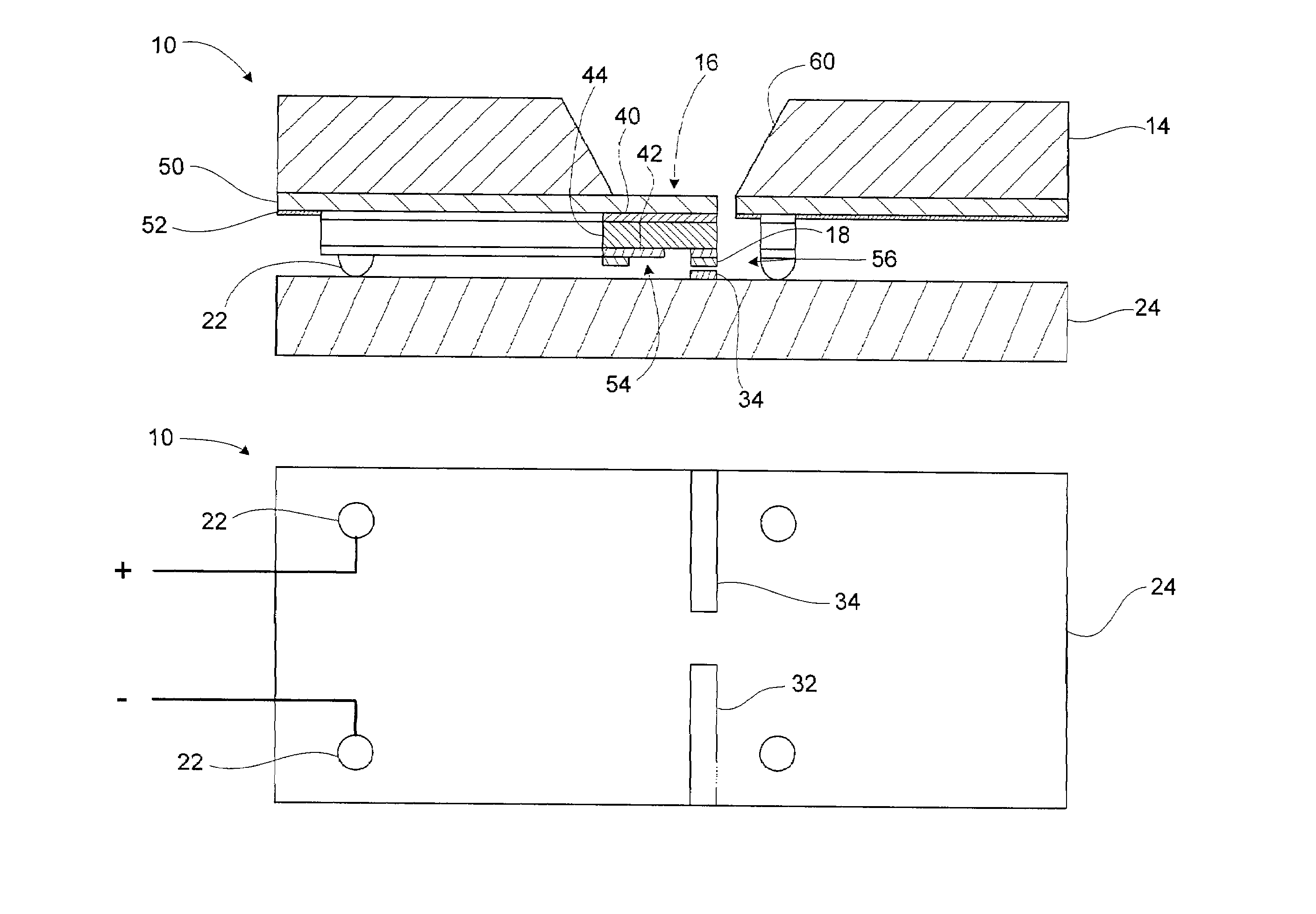
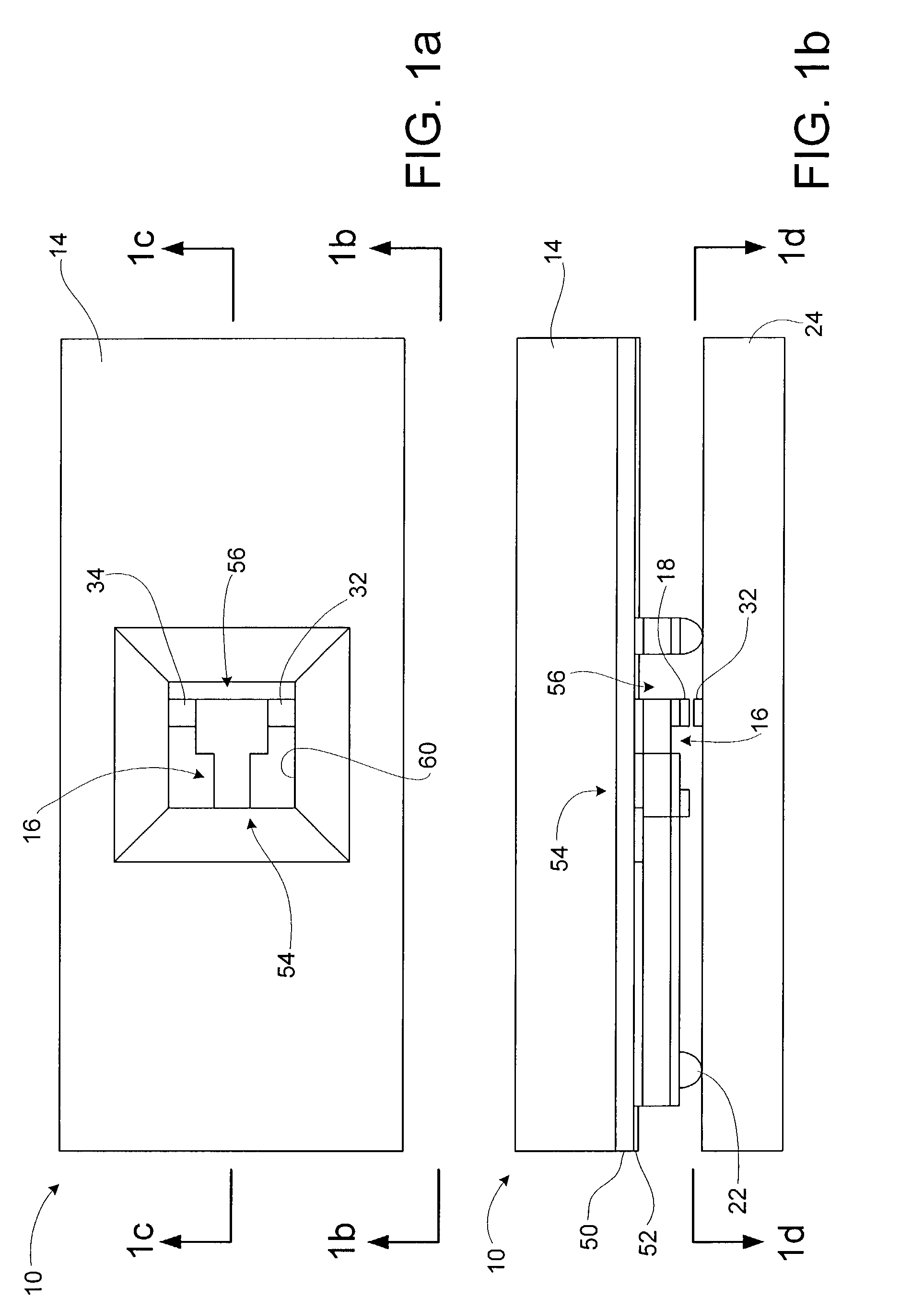
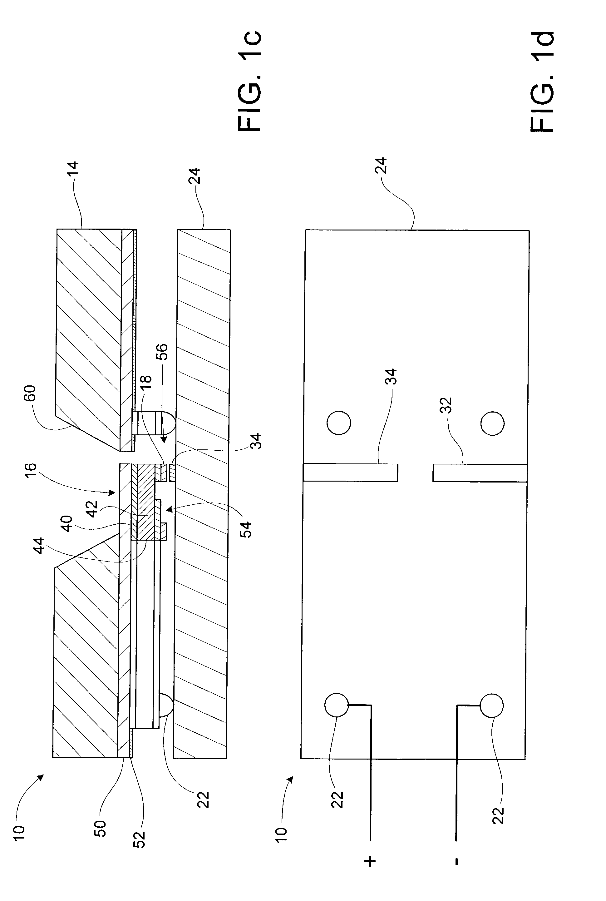
[0046]Referring initially to FIGS. 1a–1d, a radio frequency (RF) microelectromechanical system (MEMS) device 10 according to the present invention is shown. The device 10 includes a semiconductor substrate 14, a piezoelectric thin film actuator 16 mounted on the substrate 14, a conducting path electrode 18 driven by the piezoelectric thin film actuator 16, conductive bumps 22 which are connected to an external voltage source (not shown) and provide the voltage necessary for operating the device 10, an RF circuit substrate 24, and RF-in and RF-out path electrodes 32 and 34 mounted on the RF circuit substrate 24 so ...


PUM


Abstract

A radio frequency (RF) micro electro-mechanical system (MEMS) device and method of making same are provided, the device including an RF circuit substrate and an RF conducting path disposed on the RF circuit substrate, a piezoelectric thin film actuator, and a conducting path electrode. The piezoelectric thin film actuator has a proximal end that is fixed relative to the RF circuit substrate and a cantilever end that is spaced from the RF circuit substrate. The conducting path electrode is disposed on the cantilever end of the piezoelectric thin film actuator. The cantilever end of the piezoelectric thin film actuator is movable between a first position whereat the conducting path electrode is spaced from the RF path electrode and a second position whereat the conducting path electrode is spaced from the RF path electrode a second distance, wherein the second distance is less than the first distance. The RF MEMS device is particularly useful as a tunable capacitor. The RF MEMS device requires lower operating voltage, and provides variable RF tuning capacity, fewer stiction problems, simplified fabrication, and an improved switching time.

Description

TECHNICAL FIELD[0001]The present invention relates generally to micro electro-mechanical system (MEMS) radio frequency (RF) devices and methods for forming the same and, more particularly, to a tunable RF MEMS switch with a piezoelectric thin film actuator.BACKGROUND OF THE INVENTION[0002]Heretofore, radio frequency (RF) microelectromechanical system (MEMS) switches have utilized an electrostatic force or electrothermal actuation to actuate the RF MEMS switch. In a typical electrostatic RF MEMS switch, at least 30 volts may be required to open and close the switch. Consequently, the switch is not suitable for applications such as commercial handheld products, which typically operate on 3 volts or less. The electrostatic RF MEMS switch also is limited in its operation, as it can only be open or closed, that is, either in contact or not in contact. For this reason, the electrostatic RF MEMS switch is not suitable as a tunable capacitor, as such devices typically require controlled var...

Claims


Application Information

Patent Timeline
Patent Type & Authority Patents(United States)
IPC IPC(8): H01L21/00B81B3/00H01G5/16H01H57/00H01L41/24H10N30/20
CPCB81B3/0018H01G5/16H01H57/00H01L41/094H01L41/332H01H2057/006H10N30/2042H10N30/082B81B3/00
Inventor PARK, JOONNAKAHIRA, RON K.ALLISON, ROBERT C.
Owner RAYTHEON CO
Learn More