
Eureka
For R&D, Eureka makes reading and utilizing patents & technical documents easy.
Eureka AIR
Designed for self-driven R&D workflows. Generate viable solutions, solve complex R&D challenges, empower your innovation with AI.

Eureka Materials
Designed for material experts only. Revolutionize your material R&D, from search, analyze, to developing new materials.

TechResearch
Generate reliable direction feasibility study reports for your R&D in just a few steps.

TechSeek
Discover and master advanced knowledge NOW. Basics, ideas, possibilities, all at once.

TechMind
As an expert in R&D Theories, TechMind can generates customized viable solutions instantly.

TechRisk
Analyze your overall solution with one click, know your potential R&D risks in advance.

TechMonitor
Get weekly tech updates, stay abreast of the latest tech innovations and key insights.
Shallow trench isolation structure with low sidewall capacitance for high speed integrated circuits
- Summary
- Abstract
- Description
- Claims
- Application Information
AI Technical Summary
Benefits of technology
Problems solved by technology
Method used
Image

Examples
Embodiment Construction
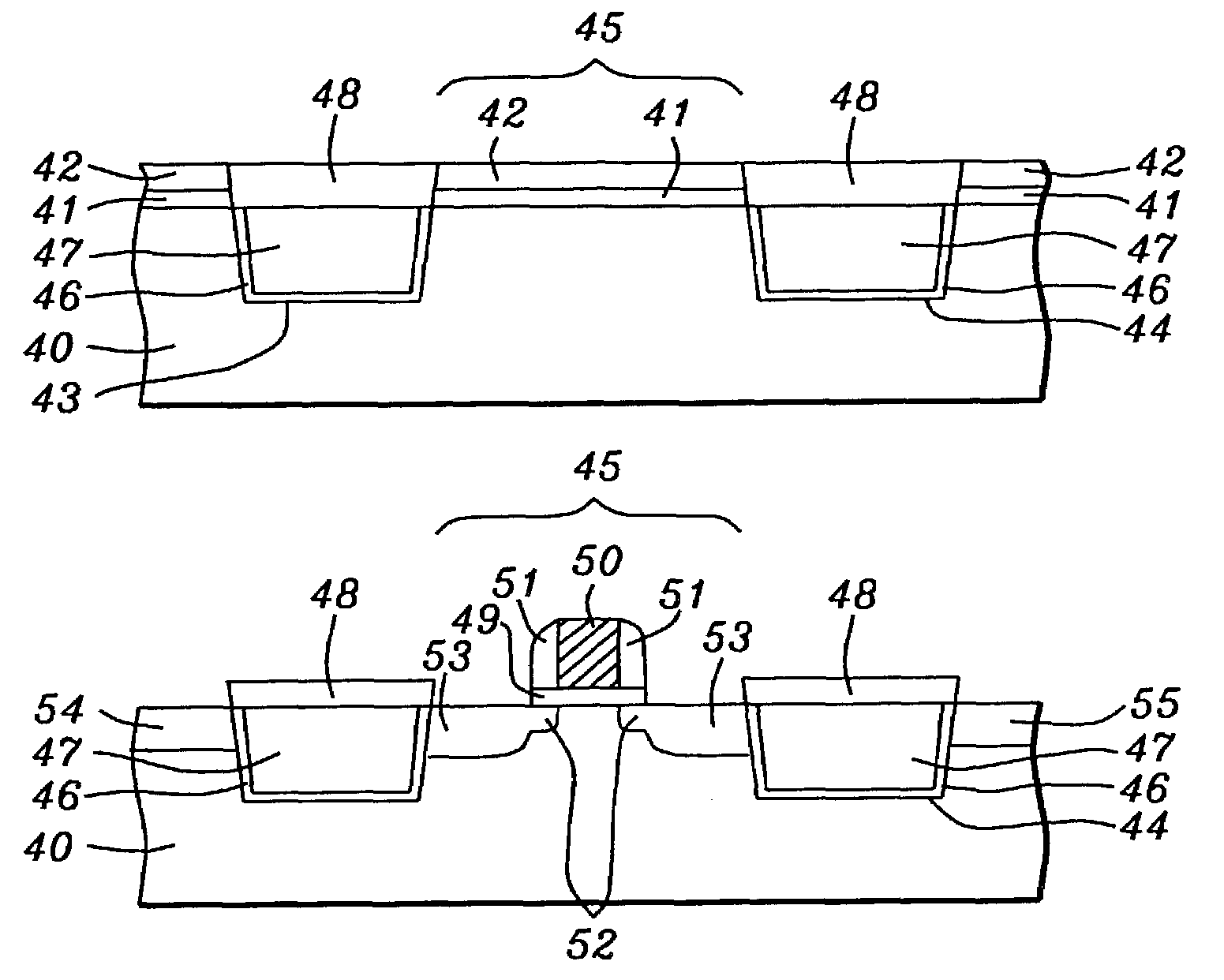
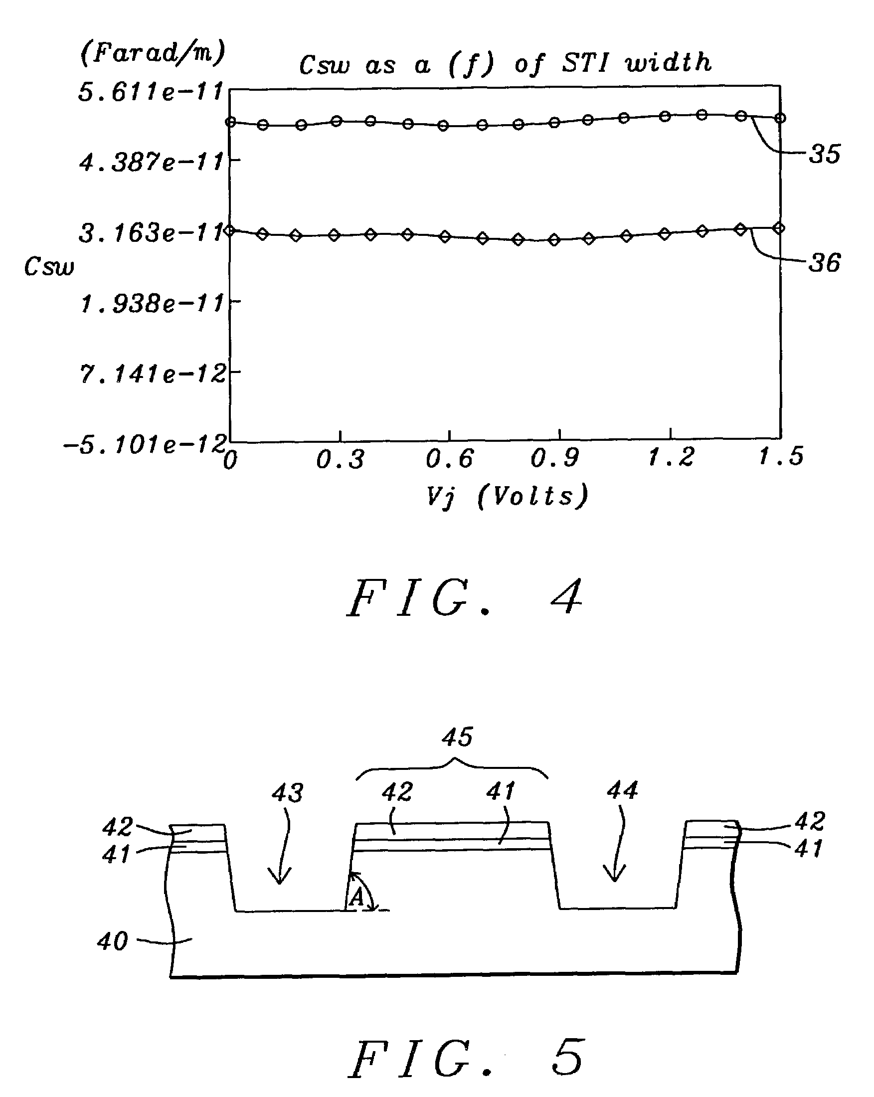
[0033]The present invention relates to a method of forming STI structures with low sidewall capacitance and having a width of less than about 0.5 microns that are used in fabricating a MOS device. The invention is also a shallow trench isolation structure with improved properties for isolating neighboring devices.
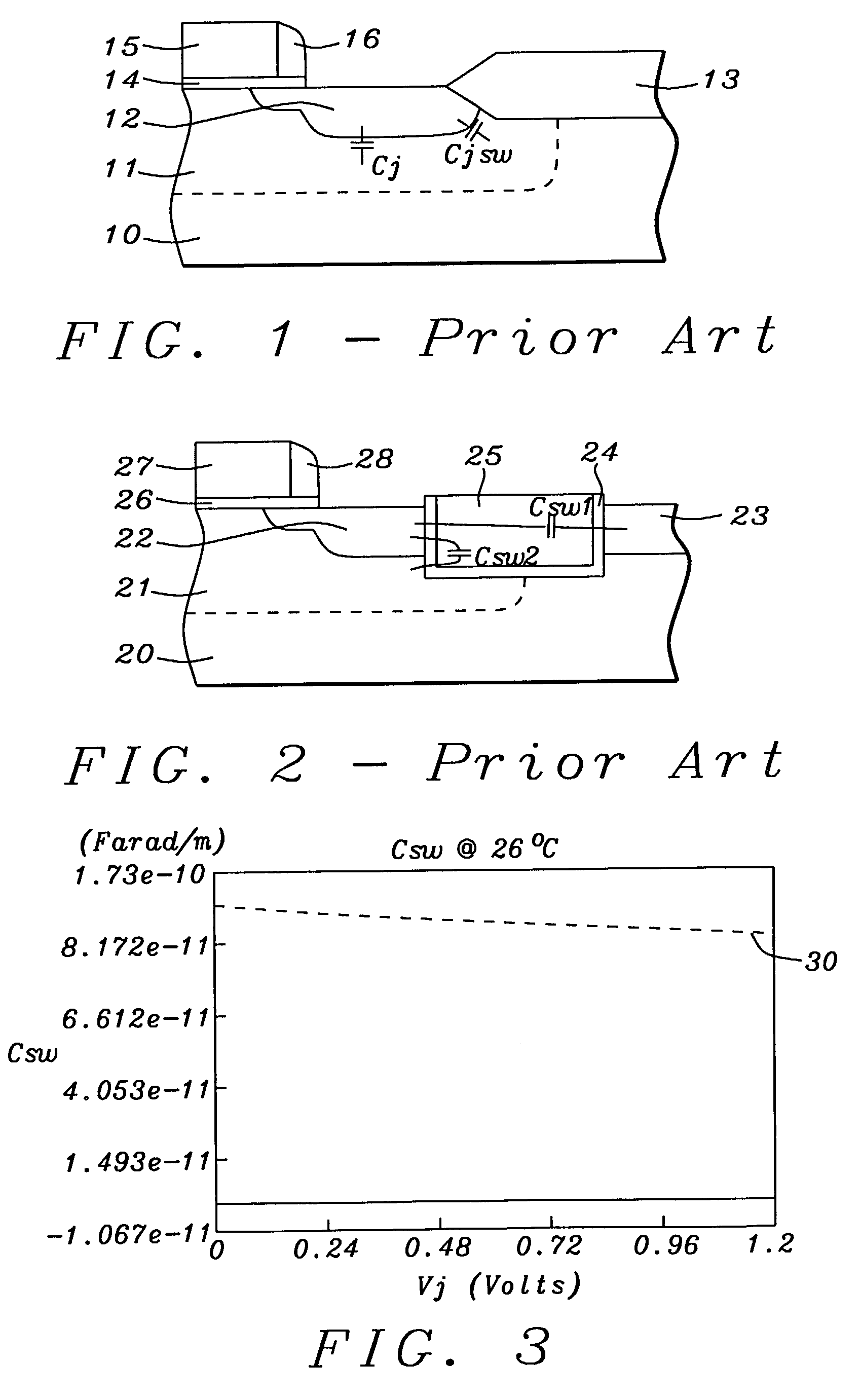
[0034]The invention will be described with reference to the drawings which are not necessarily drawn to scale. Referring to FIG. 5, a substrate 40 is provided that is typically silicon and which can be doped or undoped but may optionally be based on a silicon-germanium, gallium-arsenide, or silicon-on-insulator technology. Substrate 40 may contain a substructure (not shown) that includes active and passive devices. Trenches 43, 44 are fabricated by first depositing a pad oxide layer 41 on substrate 40. Pad oxide layer 41 may be thermally grown or deposited by a chemical vapor deposition (CVD) process. A silicon nitride layer 42 is then deposited by a CVD or plasma enhanced ...
PUM
 Abstract
Description
Claims
Application Information
 - R&D Engineer
- R&D Manager
- IP Professional
- Industry Leading Data Capabilities
- Powerful AI technology
- Patent DNA Extraction
Browse by: Latest US Patents, China's latest patents, Technical Efficacy Thesaurus, Application Domain, Technology Topic, Popular Technical Reports.
© 2024 PatSnap. All rights reserved.Legal|Privacy policy|Modern Slavery Act Transparency Statement|Sitemap|About US| Contact US: help@patsnap.com