Defect inspection instrument and positron beam apparatus

a technology of positron beam and inspection instrument, which is applied in the direction of instruments, material analysis using wave/particle radiation, nuclear engineering, etc., can solve the problems of low generating efficiency of monochromatic positron, low detection accuracy, and low probability of being trapped by an atom on the sample surface. achieve sufficient resolution, and reduce the intensity of positron beam

Inactive Publication Date: 2006-11-28
HITACHI LTD
View PDF6 Cites 4 Cited by
  • Summary
  • Abstract
  • Description
  • Claims
  • Application Information

AI Technical Summary

Benefits of technology

[0019]It is an object of the present invention to provide a solution for compatibility of resolution and sensitivity by detecting γ-rays which are generated by irradiation of a positron beam and converging the electronic beam against a sample. As described above, monochromaticity drastically lowers the intensity of a positron beam. However, in the case of an electron beam, techniques such as monochromatic electron beams and converging electromagnetic coils have been developed, therefore it is possible that the spot diameter of a beam can be made smaller while maintaining a practical electron beam intensity. Then, in this invention, positrons are irradiated onto a relatively wide area of sample and a converging electron beam is simultaneously irradiated onto the sample. With this method it is possible to control the size of the area generated by γ-rays to almost the order of the beam spot diameter of the converging electron beam, and it is also possible to provide sufficient resolution compared with the prior art. Moreover, the problem of reduced positron beam intensity due to the absence of monochromaticity does not appear. Therefore, the decrease in the intensity of generated γ-rays can be made smaller than the prior art, resulting in realizing the compatibility of resolution and sensitivity within a practical range.

Problems solved by technology

When an evaluation method using positrons is applied to defect inspection of a semiconductor sample, the detectable size of defects is a problem.
However, a positron has the characteristic of obtaining an energy equal to the work function on the sample surface, therefore it has a low probability of being trapped by an atom on the sample surface.
However, the generating efficiency of a monochromatic positron is low because of a low re-emission probability of about 10−4.
However, for example, in an electrical device such as a semiconductor memory, wherein a transistor gate length and circuit structure of one bit which is the smallest unit of structure is less than 10 nm (in some cases, several nanometers), and when knowledge of the internal distribution is desired, realizing a spatial resolution less than 1 nanometer is required, and the problem occurs that the spatial resolution is inadequate by one to three orders of magnitude.
However, monochromaticity makes the positron intensity about 1000 to 100000 times weaker than the positron intensity as emitted from the source, therefore the signal intensity of detected γ-rays becomes weaker, thereby creating a problem of inadequate measurement sensitivity.
Measurements using an accelerator as a source have been attempted experimentally to maintain positron intensity, but there are problems such as cost and limitations on the number of measurements.
It is therefore difficult to apply it to civilian products such as semiconductor devices.

Method used


Image

  • Defect inspection instrument and positron beam apparatus
  • Defect inspection instrument and positron beam apparatus
  • Defect inspection instrument and positron beam apparatus

Examples


first embodiment

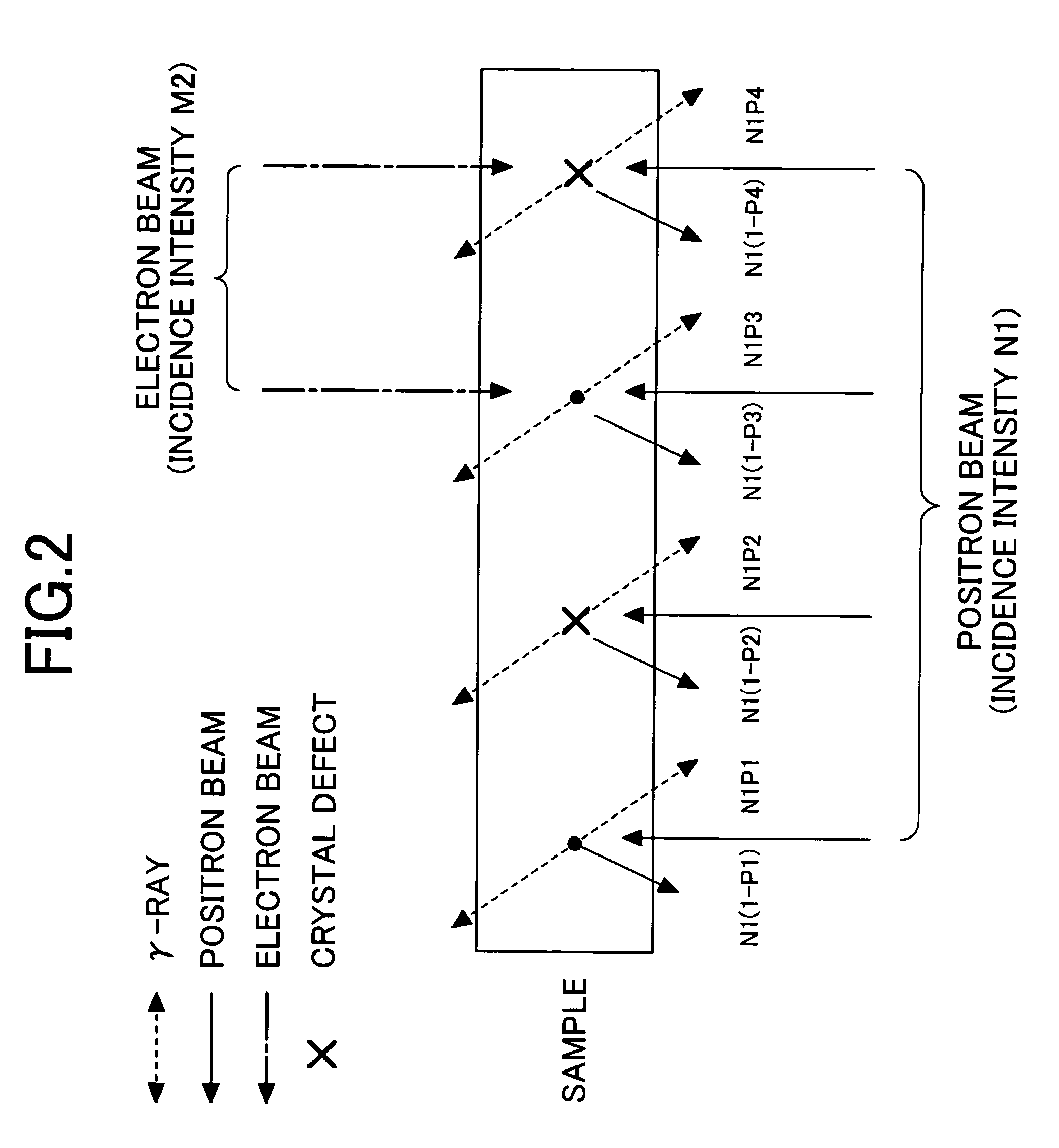
[0026]First, the principle of a defect number measurement method is described using FIG. 2. In this figure, four cases are described. That is, it means four kinds of combinations of samples, with or without defects, and injection of only electron beams or both electron and positron beams onto the sample. Positrons injected into the sample lose energy in the sample by repeated inelastic scattering. The low-energy positrons pair-annihilate with electrons in the sample. It means that they disappear radiating usually two streams of 511 keV γ-rays. Additionally, there are positrons, not pair-annihilated, which are re-emitted outside the sample. Herein, when the electron intensity injected into a sample is N1 and the probability of pair annihilation with an electron is p1 (0P1, C1>1. A method described in the prior art uses a method, wherein this ratio c1 is principally detected as a contrast.

[0027]On the other hand, considering the case when both positrons and electrons are simultaneousl...

second embodiment

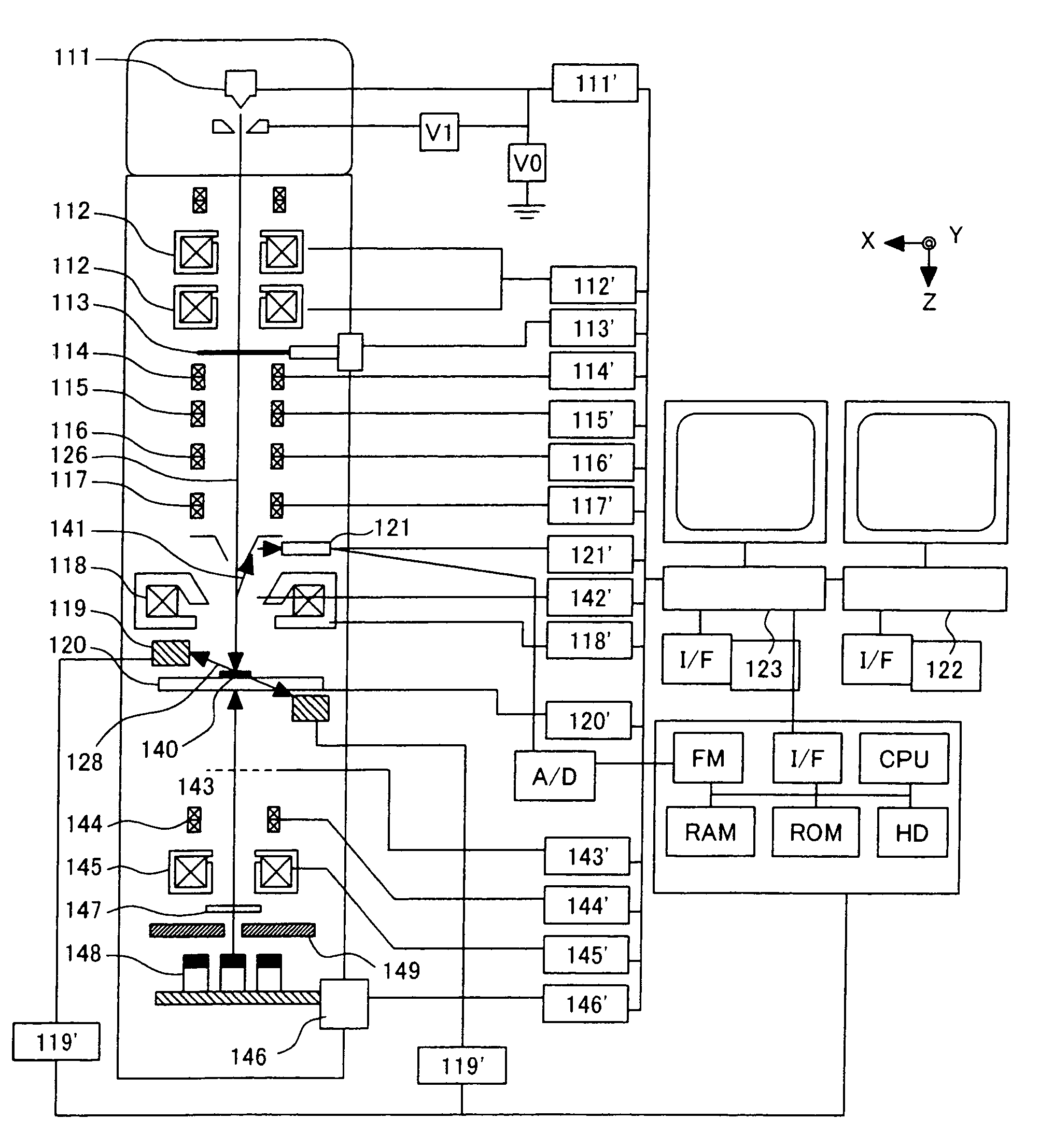
[0042]FIG. 4 shows the second example. The point irradiating the positron beam from the right side of the sample and the converging electron beam from the left side of the sample is similar to the first example of FIG. 1. In this example, to maintain convergence by as low acceleration as possible, a deceleration mesh 18, that decelerates the accelerating electron beam immediately before the sample, was installed. A decelerating voltage 19 of opposite sign to the extraction voltage 5 and accelerating voltage 6 was applied on this deceleration mesh. It is necessary that the sample be at a low enough energy to generate the pair annihilation with the positron. Moreover, in order to suppress incident electron beam spreading by scattering inside the sample it is effective to make an electron beam with low energy. Rather than convergence by means of an electromagnetic coil 3 at a low accelerating voltage, convergence is maintained by deceleration after adequately established at high accele...

third embodiment

[0044]In a semiconductor device in recent years, the probability of creating a micro-defect, which is invisible with the prior art, in a substrate or circuit pattern formed on a substrate, is increasing because of introducing new structures such as adoption of an SOI (Silicon on insulator) wafer containing an oxide film layer inside. Because such micro-defects cause a junction current leakage, evaluation of point defects and micro-defects in the crystal (presence, density and position identification etc.) becomes more important. For example, image contrast cannot be observed by a Transmission Electron Microscope (TEM) if the defect does not exist in a ratio greater than or equal to unity for five nascent atomic rows. That is, it was necessary to make the sample thickness less than 1 nm and to condense several defects, otherwise evaluation of the above-mentioned point defects in a solid material or cluster defects consisting of two or more defects were difficult using a conventional ...


PUM

PropertyMeasurementUnit
energyaaaaaaaaaa
lengthaaaaaaaaaa
acceleration voltageaaaaaaaaaa

Abstract

The purpose of the present invention is to inspect the position, number, and size of fine defects in a variety of solid state materials, including a semiconductor device and metallic materials, with a high spatial resolution of nanometer order. The positron irradiation function is installed in the converged electron beam apparatus. The defect location information is obtained from the converged electron beam location information, and the number and size of defects are obtained from the detected information of γ-rays created by pair annihilation of electrons and positrons, and this two-dimensional distribution information is displayed in the monitor. Information on ultra-fine defects in a crystal can be provided with high-speed and high-resolution, and nondestructively in the case of a semiconductor wafer.

Description

CLAIM OF PRIORITY[0001]The present application claims priority from Japanese application JP 2003-135265 filed on May 14, 2003, the content of which is hereby incorporated by reference into this application.FIELD OF THE INVENTION[0002]This invention relates to an inspection instrument, in which the position, number and size of micro-defects are detected in various kinds of solid state materials including a semiconductor device and a metallic material using electron beams and positron beams.BACKGROUND OF THE INVENTION[0003]Recently, positrons have received attention as a technology to detect micro-defects in a semiconductor device. Although a positron has a mass almost equal to that of an electron and a positive electric charge opposite to that of an electron, it does not exist stably in the natural world because the lifetime is as short as several-hundred picoseconds (one picosecond means 10−12 seconds), but it can be generated by a nuclear reaction. Defects in a material are negativ...

Claims


Application Information

Patent Timeline
Patent Type & Authority Patents(United States)
IPC IPC(8): G01N23/00G01N23/225G21K7/00G01N23/22G01T1/161G01T1/172G21K1/00G21K5/00G21K5/04H01J37/147H01J37/256H01J37/26H01J37/28
CPCG01N23/2252H01J37/256H01J37/26H01J2237/2807
Inventor KOGUCHI, MASANARITSUNETA, RURIKO
Owner HITACHI LTD
Why Eureka
Try Eureka