High voltage transistor having side-wall width different from side-wall width of a low voltage transistor

Inactive Publication Date: 2006-12-12
SHARP KK
View PDF3 Cites 2 Cited by
  • Summary
  • Abstract
  • Description
  • Claims
  • Application Information

AI Technical Summary

Benefits of technology

[0022]The manufacturing method for a semiconductor device according to the present invention, when forming the side walls the widths of that are difference, in its preferred embodiment, has a step of, with the stopper film consisting of a high selectivity silicon nitride film being formed, beforehand, as the lower layer of, and inside, the side walls of the low voltage transistor region, eliminating the side walls consisting of a silicon oxide film with use of isotropic etching that is thereafter performed. As a result of this, by structuring in such a way that the relevant transistors of different breakdown voltage specifications have side walls whose widths are different from each other, on the high breakdown voltage transistor side the breakdown voltage performance becomes again higher while on the low voltage transistor side the parasitic resistance becomes small, whereby a high driving electric current is ensured. In addition, for that reason, reducing the element in size becomes possible. As a result of that, it is possible to obtain a semiconductor device that has excellent element isolat

Problems solved by technology

However, in the above-described conventional method, in a case where the non-volatile semiconductor memory device and low voltage logic circuit have been co-loaded on the same one chip, the following inconvenience arises.
Namely, when eliminating the first side wall film in the low voltage transistor region, since there is not the stopper film, or the like, that protects the element isolation insulative film, it is in actuality difficult, regarding stopping etching at the position of element isolation insulative film, to perform control for that stopping.
This raised the problem that, during the manufacturing process steps, the element isolation insulative film was excessively et

Method used


Image

  • High voltage transistor having side-wall width different from side-wall width of a low voltage transistor
  • High voltage transistor having side-wall width different from side-wall width of a low voltage transistor
  • High voltage transistor having side-wall width different from side-wall width of a low voltage transistor

Examples


first embodiment

(First Embodiment)

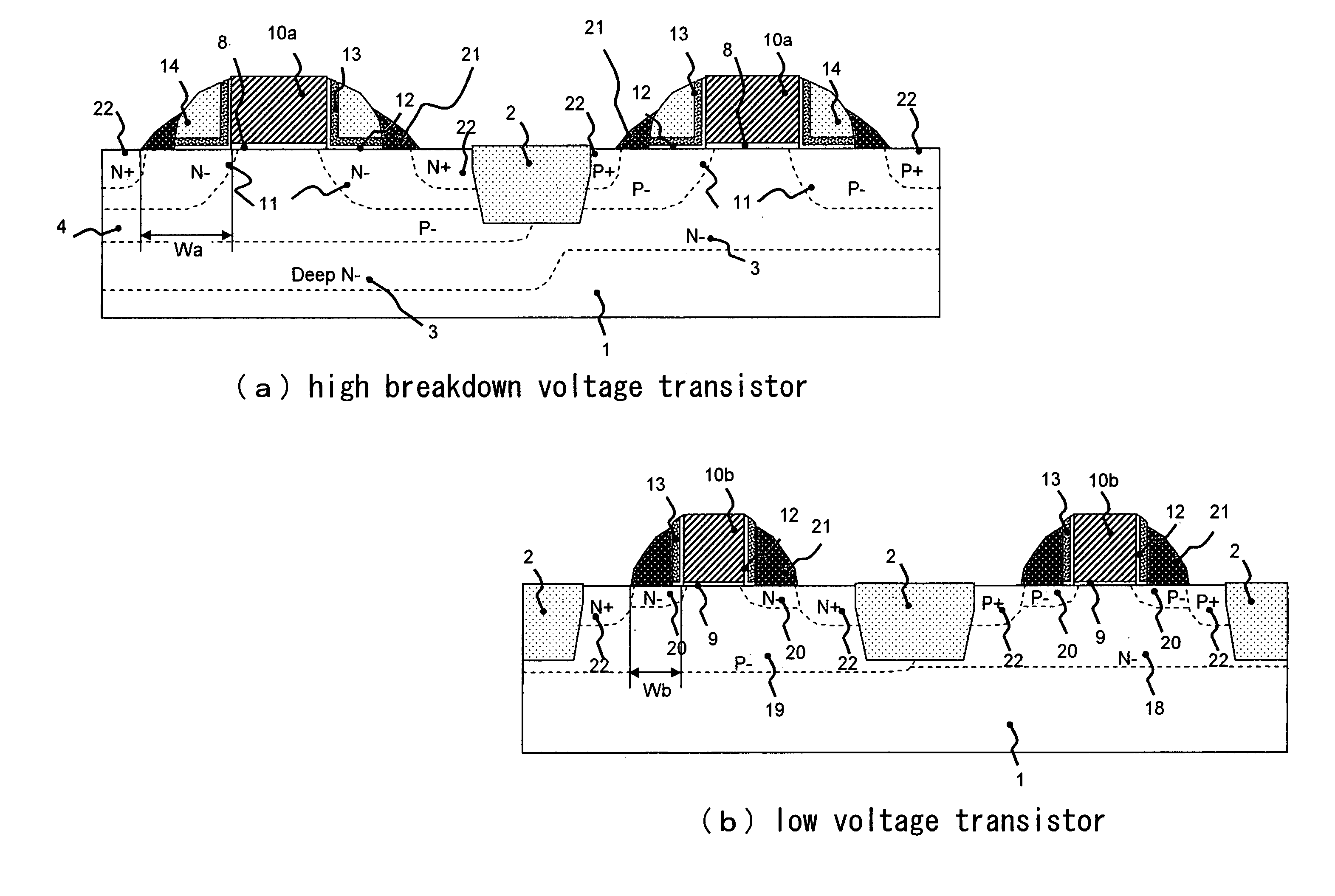
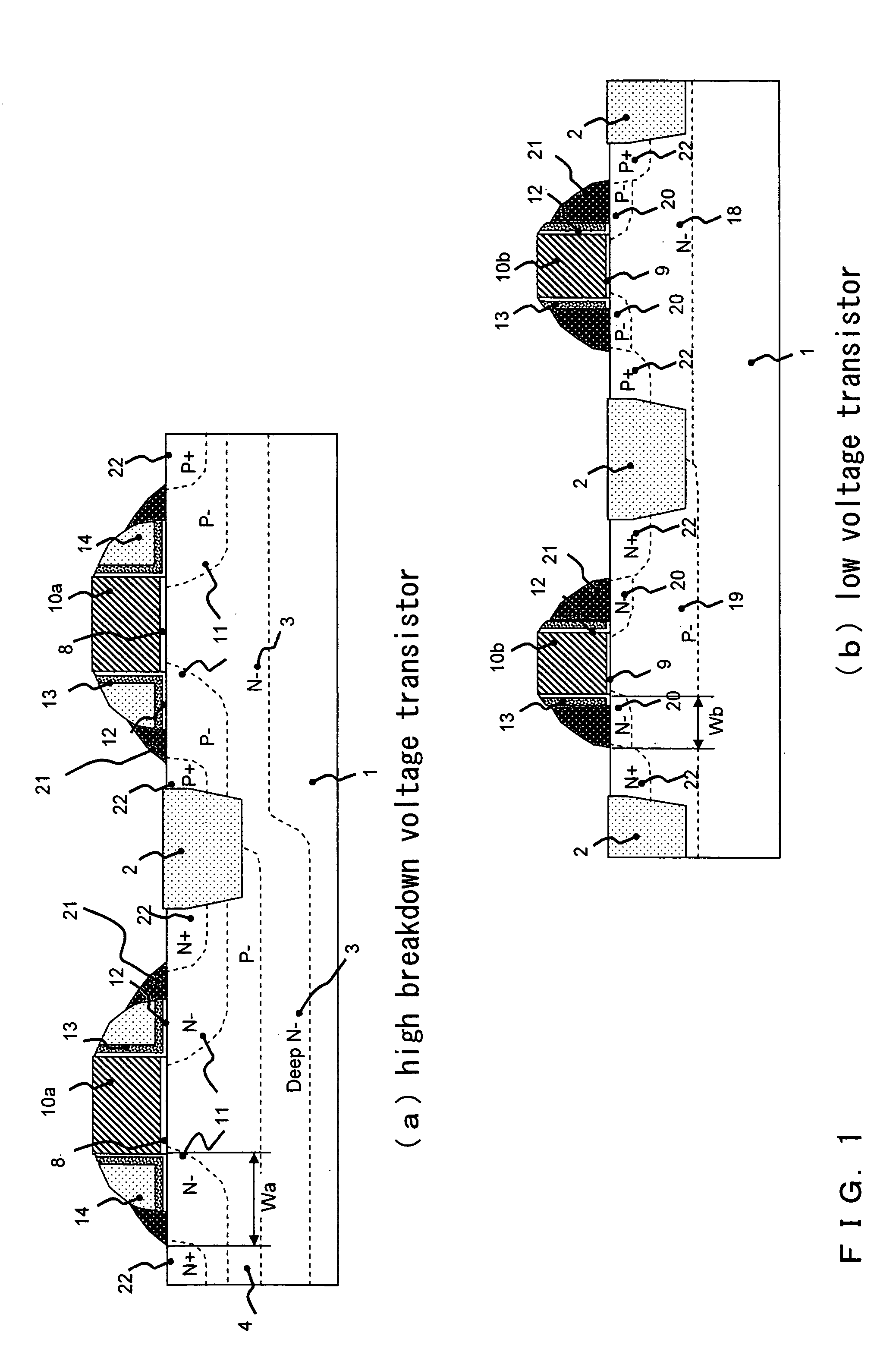
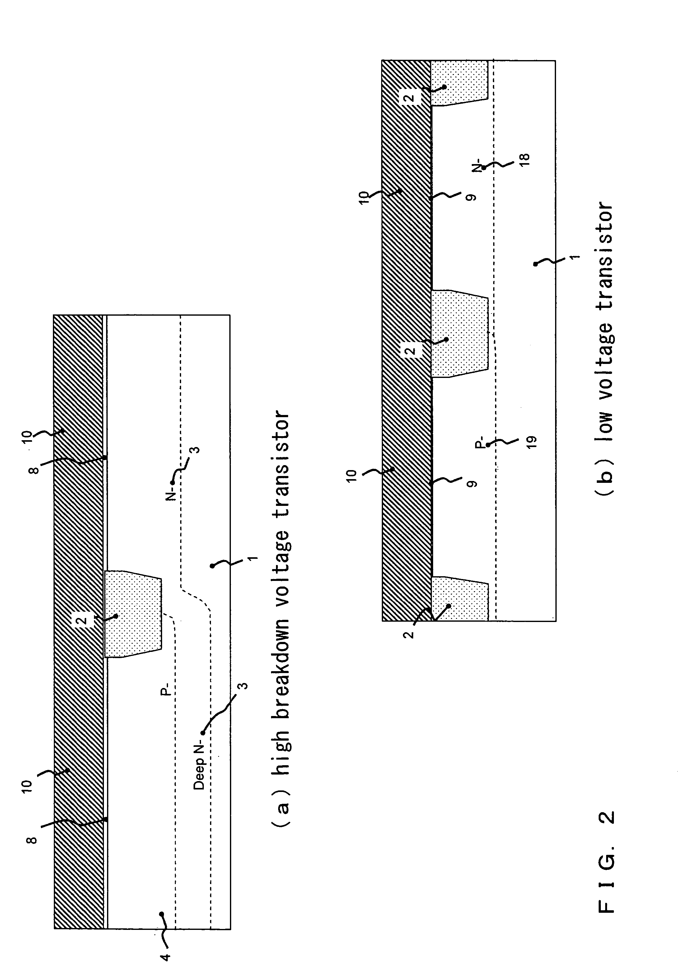
[0039]In FIGS. 1(a) and 1(b), there are shown respective sectional structures of a high breakdown voltage transistor and low voltage transistor of the invention device. FIG. 1 illustrates an example wherein the invention has been applied to a co-loaded device wherein the high breakdown voltage transistor circuit and a high-speed logic circuit are co-loaded. Incidentally, in FIG. 1, the left side is the high breakdown voltage transistor (a) and the right side is the low voltage transistor (b). Also, in the FIGS. 1(a) and 1(b), the contact holes for having metal interconnection performed with respect to the source / drain electrodes of each of the transistors, the metal interconnection layer, the interlayer insulation films, the protective films, etc. are description omitted.

[0040]In the high breakdown voltage transistor (a), as the side wall of a gate electrode 10a, there are sequentially laminated from each of both side surfaces of the gate electrode 10a in the direc...

second embodiment

(Second Embodiment)

[0059]Although in the above-described first embodiment an explanation has been given of a case where there exist two types of transistors the widths of whose side walls are different, i.e. the high breakdown voltage transistor (a) and low voltage transistor (b), the invention device and invention method can also be applied in a case where, in addition to the high breakdown voltage transistor (a) and low voltage transistor (b), there is provided a floating gate type memory cell transistor for use for a non-volatile semiconductor memory, with the result that the resulting semiconductor device has co-loaded therein the non-volatile semiconductor memory such as a flash memory.

[0060]Here, if process steps for forming a memory cell transistor are suitably inserted into between after the execution of the side wall forming steps (the above-described third series of process steps) for the first to third side wall films 12, 13, and 14 of the high breakdown voltage transisto...

third embodiment

(Third Embodiment)

[0062]In each of the above-described first and second embodiments, as the side walls of the high breakdown voltage transistor (a), the four layers of the silicon oxide film (the first side wall film 12), silicon nitride film (the second side wall film 13), silicon oxide film (the third side wall film 14), and silicon oxide film (the fourth side wall film 21) have been formed in the way of being sequentially laminated, and as the side walls of the low voltage transistor (b), the three layers of silicon oxide film (the first side wall film 12), the silicon nitride film (the second side wall film 13), and silicon oxide film (the fourth side wall film 21) have been formed in the way of being sequentially laminated. However, in the side walls of each of the high breakdown voltage transistor (a) and low voltage transistor (b), providing the silicon oxide film (the first side wall film 12) is not always needed. In this case, since the thickness of the silicon oxide film (...


PUM


Abstract

The present invention has an object to provide a semiconductor device that is equipped with a high breakdown voltage transistor of a high junction breakdown voltage characteristic and a low voltage transistor of a high electric current drive characteristic to thereby ensure the element isolation performance in the both transistor forming regions. The semiconductor device is equipped with a high breakdown voltage transistor (a) and low voltage transistor (b) the widths of whose side walls are different from each other. The side walls of the high breakdown voltage transistor (a) each consist of four layers of first side wall film, second side wall film, third side wall film, and fourth side wall film that are formed in such a way that they are laminated from both side surfaces of a gate electrode in directions that are sidewardly remote away from this gate electrode. The side walls of the low voltage transistor (b) each consist of three layers of the first side wall film, the second side wall film, and the fourth side wall film that are formed in such a way that they are laminated from both side surfaces of a gate electrode in directions that are sidewardly remote away from this gate electrode.

Description

BACKGROUND OF THE INVENTION[0001]1. Field of the Invention[0002]The present invention relates to a semiconductor device that is equipped with a high breakdown voltage transistor and a low voltage transistor, the side wall widths of which are different from each other and a method of manufacturing the same. More particularly, the invention concerns a semiconductor device wherein a high voltage drive circuit and a low voltage drive circuit are co-loaded on the same chip and a method of manufacturing the same. Further, the invention concerns a semiconductor device wherein a non-volatile memory cell array is integrated and a method of manufacturing the same.[0003]2. Description of the Related Art[0004]There has in recent years been an increasing demand for a semiconductor integrated circuit wherein, together with a non-volatile memory cell array, a logic circuit that is driven with a high speed is co-loaded on the same chip to thereby enhance the added value.[0005]In this type of semico...

Claims


Application Information

Patent Timeline
IPC IPC(8): H01L29/00H01L21/336H01L21/8234H01L21/8238H01L21/8247H01L27/088H01L27/092H01L27/10H01L27/115H01L29/78H01L29/788H01L29/792
CPCH01L21/823418H01L21/823456H01L21/823468H01L21/823814H01L21/82385H01L21/823864H01L27/0922Y10S257/90
Inventor FUJIO, MASAYUKIARIMURA, MOTOHARU
Owner SHARP KK
Why Eureka
Try Eureka