Progressive self-learning defect review and classification method

a self-learning and defect technology, applied in the field of progressive self-learning wafer defect review and classification method, can solve the problems of long mask writing time, lack of hardware development in mask inspection, and long conversion time for fracturing, so as to accelerate the timing of the classification process and reduce the loading time of operators

Active Publication Date: 2007-01-09
TAIWAN SEMICON MFG CO LTD
View PDF2 Cites 40 Cited by
  • Summary
  • Abstract
  • Description
  • Claims
  • Application Information

AI Technical Summary

Benefits of technology

[0021]Successful implementation of the PSL method to classify mask or wafer defects will reduce an operator's loading time and accelerate the timing of the classification process. Also, the PSL method will automatically classify same type of defects without the need for

Problems solved by technology

Aggressive OPC correction lengthens a conversion time for fracturing and prolongs a mask writing time.
Existing OPC corrected layout systems and methods challenge wafer/mask inspection capability.
In addition, a lack of hardware development in mask inspection has turned mask inspection into a bottleneck in the wafer fabrication process.
Thus, a full automation inspection method is infeasible using existing mask inspection tools.
Wafer/mask defect inspection, particularly, wafer/mask defect review and classification, is time consuming, tedious work requiring an operator's manual assistance.
However, as a defect number increases above 100, defect classification becomes time-consuming, thus, prolonging the mask-making cycle time.
With a moderate increase of defects,

Method used


Image

  • Progressive self-learning defect review and classification method
  • Progressive self-learning defect review and classification method
  • Progressive self-learning defect review and classification method

Examples


Embodiment Construction

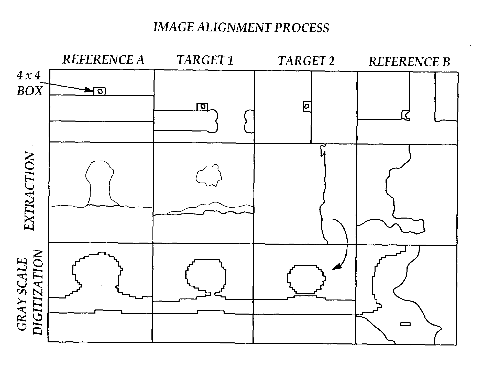
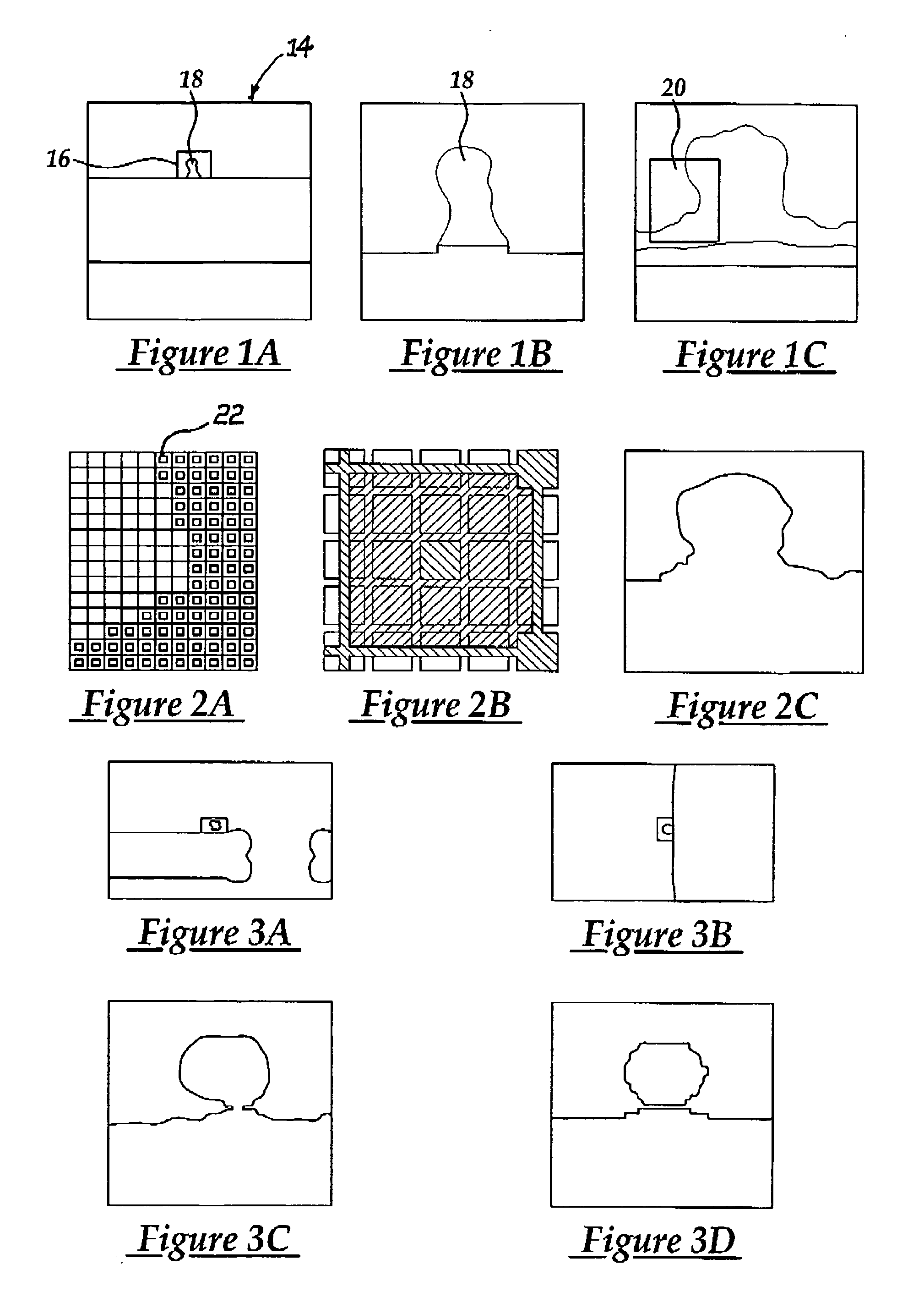
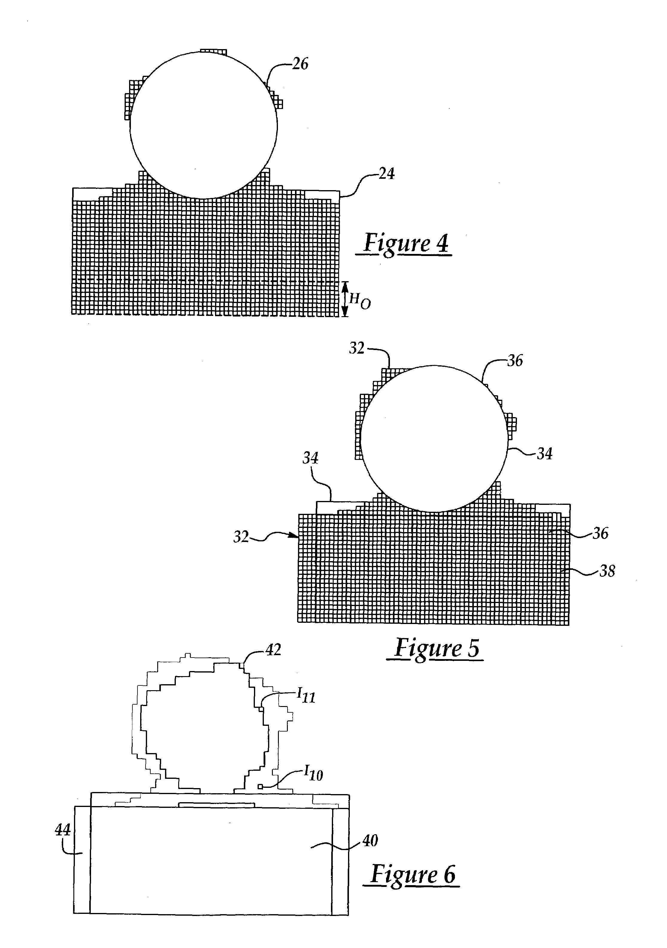
[0043]The present invention provides a progressive self-learning (PSL) method for enhancing wafer or mask defect review and classification by identifying a plurality of photomask or wafer defects, and classifying each of the plurality of defects according to an extent of resemblance of each defect.

[0044]Successful implementation of the PSL method to classify mask or wafer defects will reduce an operator's loading time and accelerate the timing of the classification process. Also, the PSL method will automatically classify same type of defects without the need for additional human intervention. The PSL method is particularly beneficial for use in a stage of wafer or mask process developing, wherein repetitious types of defects are frequently observed. The PSL method also provides a step for automatically categorizing nuisance defects.

[0045]The PSL method of the present invention performs five basic steps to enhance the efficiency and accuracy of a wafer or mask defect review and defe...


PUM


Abstract

A progressive self-learning (PSL) method is provided for enhancing wafer or mask defect inspection review and classification by identifying a plurality of wafer or mask defects, and by classifying each of the plurality of defects according to an extent of resemblance of each defect. The method having the steps of: performing image processing on a scanned defect image; aligning the scanned defect image with a just-stored digitized defect image; matching the scanned defect image with a just-stored digitized defect image; and classifying the scanned defect image.

Description

FIELD OF THE INVENTION[0001]The present invention is directed to a progressive self-learning wafer defect review and classification method for enhancing a defect inspection process in a wafer fabrication facility.BACKGROUND[0002]An existing method for reviewing and classifying wafer / mask defects is a mandatory manual task using existing hardware configurations in current wafer manufacturing environments. The need for advanced mask-making and wafer fabrication capability grows as the demand for semiconductor technology having small features increases. Optical proximity correction (OPC) is becoming a standard procedure for printing deep subwavelength features in current wafer / mask manufacturing. Data preparation and data handling require file size expansion using OPC corrected layouts. Aggressive OPC correction lengthens a conversion time for fracturing and prolongs a mask writing time. Existing OPC corrected layout systems and methods challenge wafer / mask inspection capability. In ad...

Claims


Application Information

Patent Timeline
IPC IPC(8): G06K9/00G06T7/00
CPCG06T7/001G06T2207/30148
Inventor HUNG, CHANG-CHENGHSU, TYNG-HAOLIN, CHIN-HSIANGLIN, CHUAN-YUANCHEN, SHIN-YING
Owner TAIWAN SEMICON MFG CO LTD
Why Eureka
Try Eureka