Supercharge Your Innovation With Domain-Expert AI Agents!

Optical element and method for its manufacture as well as lithography apparatus and method for manufacturing a semiconductor device

Inactive Publication Date: 2007-02-06
CARL ZEISS SMT GMBH
View PDF30 Cites 19 Cited by
  • Summary
  • Abstract
  • Description
  • Claims
  • Application Information

AI Technical Summary

Benefits of technology

[0017]It is the object of the present invention to provide an optical element, which by reducing contamination provides as long a service life as possible with the best possible constant reflectivity, and which can make contribution to reducing the cost of lithography apparatus, and to reducing the production costs of semiconductor devices.

Problems solved by technology

With photomasks, too, contamination is a big problem, because the structures to be imaged are no longer in focus as a result of deposits e.g. of carbon.
Furthermore, there are irradiation and heat effects which negatively affect the reflectance at “operating wavelength”.
On the other hand, matching of the wavelength leads to operation outside the operating wavelength, which in turn leads to loss of reflectance.
However, any other contamination of the mirror, apart from oxidation, is only suppressed insignificantly or is not suppressed at all.
As a consequence, damage such as high tension or cracks resulting from excessive irradiation load (approx.

Method used


Image

  • Optical element and method for its manufacture as well as lithography apparatus and method for manufacturing a semiconductor device
  • Optical element and method for its manufacture as well as lithography apparatus and method for manufacturing a semiconductor device
  • Optical element and method for its manufacture as well as lithography apparatus and method for manufacturing a semiconductor device

Examples


Embodiment Construction

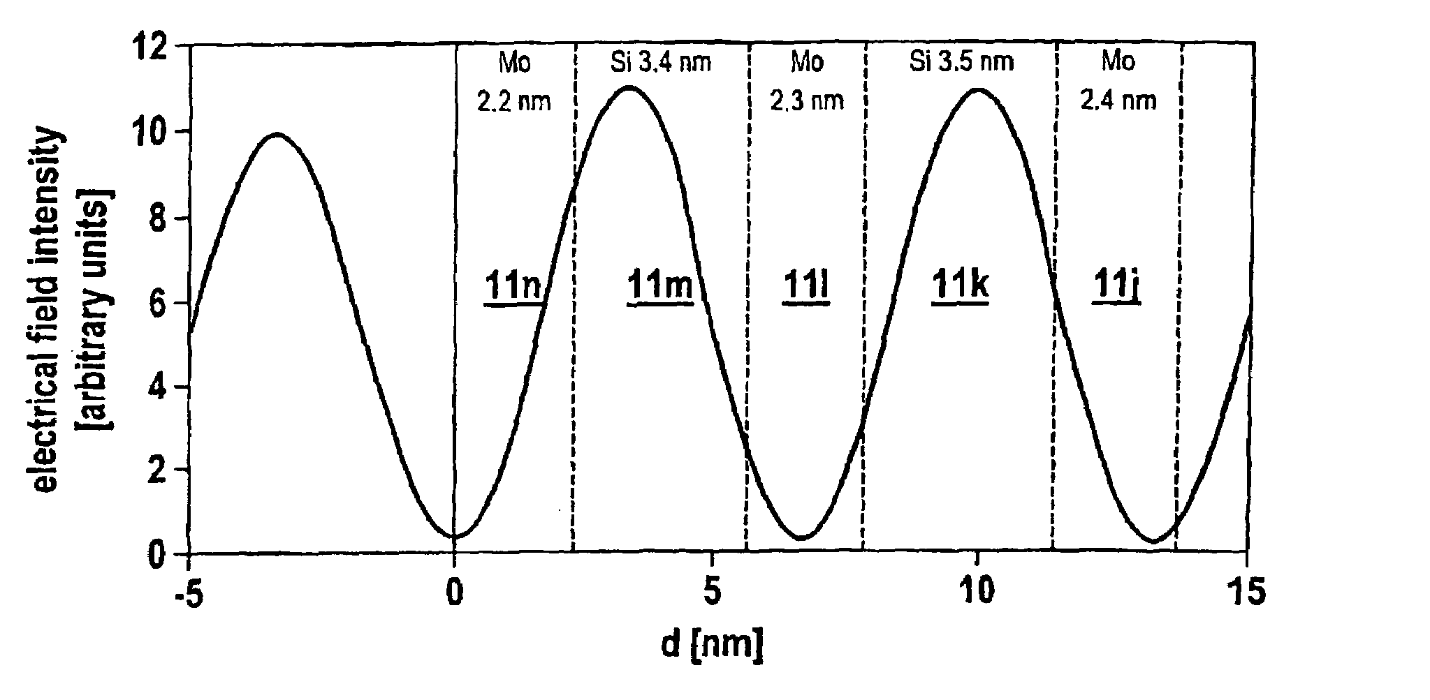
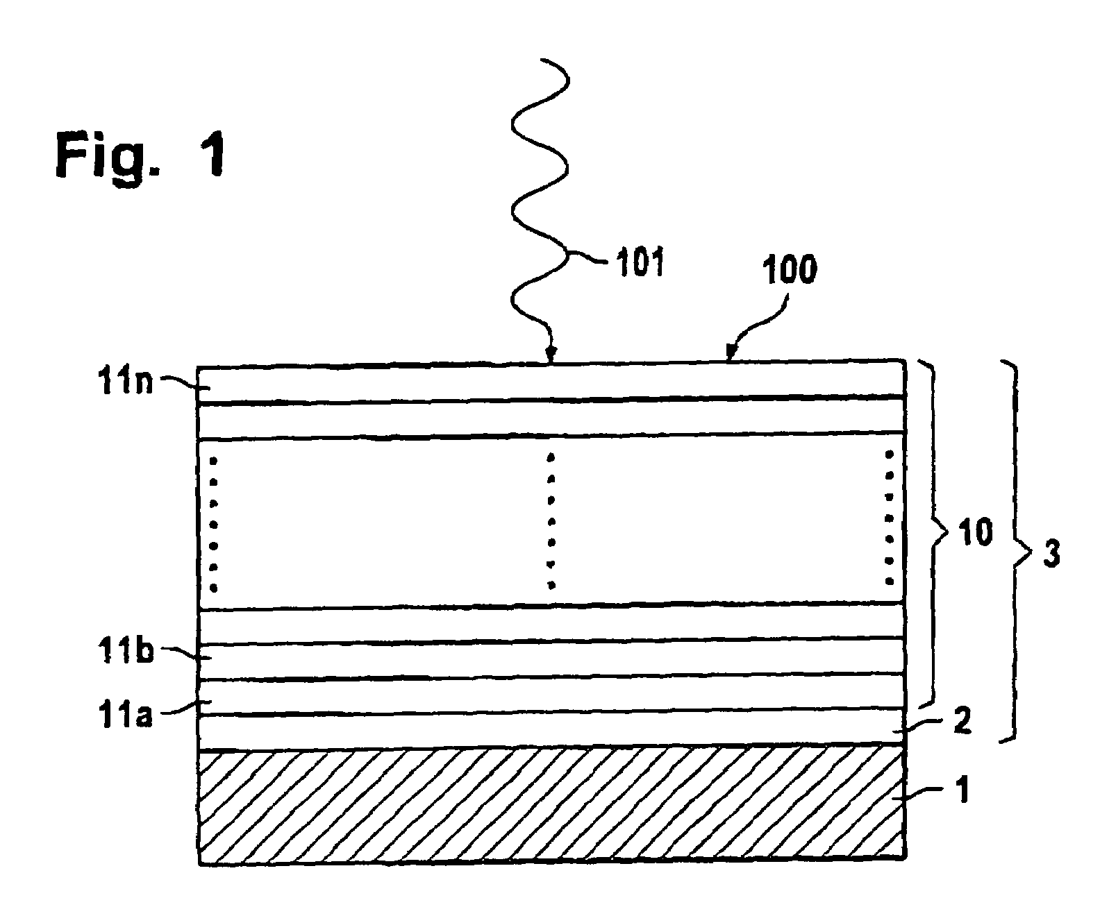
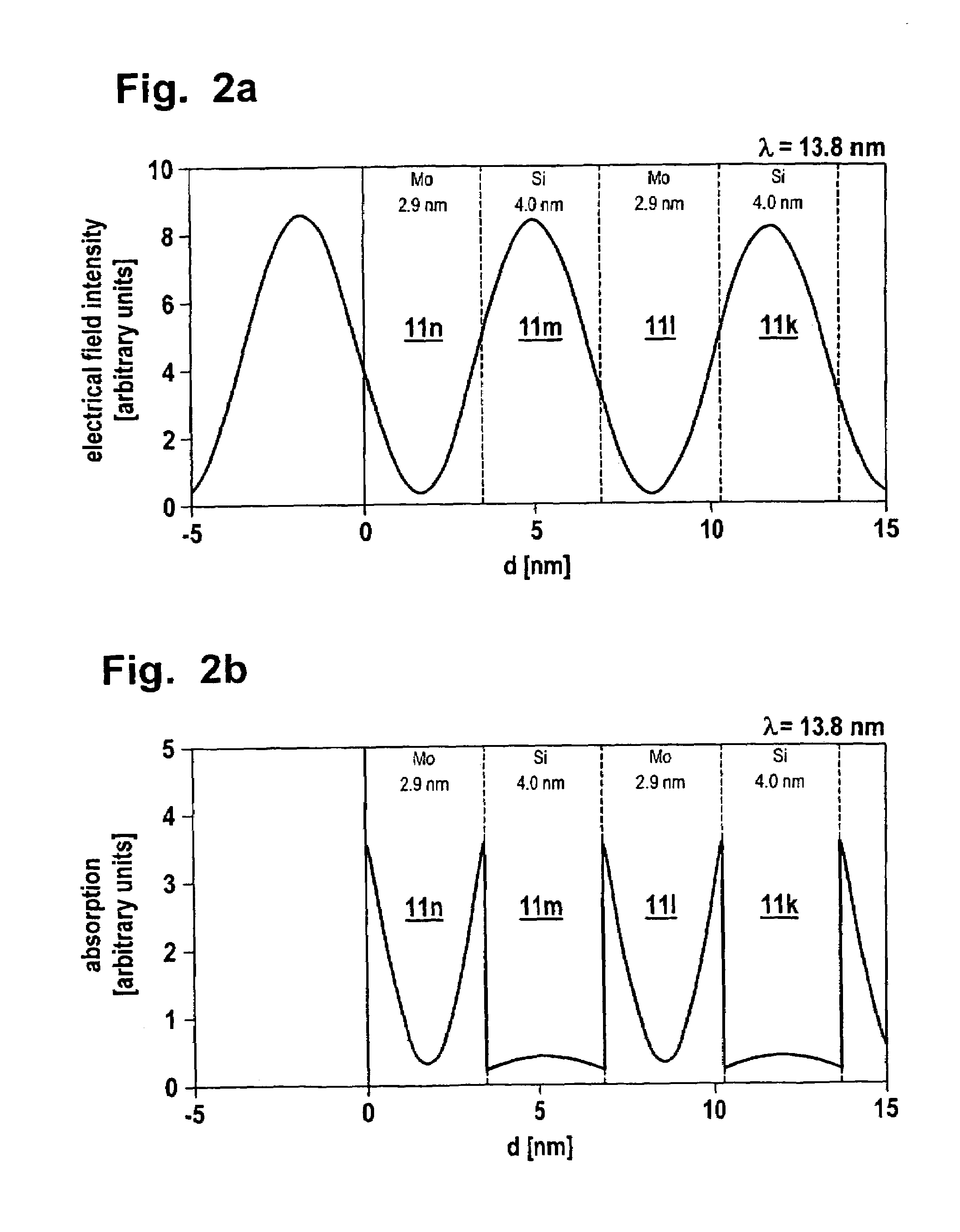
[0075]FIG. 1 shows an optical element comprising a substrate 1, buffer section 2 and a resonance section 10, wherein the buffer section 2 and the resonance section 10 with the layers 11a to 11n constitute the multilayer system 3. Electromagnetic radiation 101 is directed onto the free interface 100.

[0076]For example Zerodur® (Schott), Clearceram® (Ohara), fused silica, silicon and ULE® (Corning), can be used as substrate materials. It is not always possible to polish the substrate 1 to the required 0.1 nm microroughness. Therefore the so-called buffer section 2 is used for additional substrate smoothing or substrate preparation prior to the actual coating, i.e. prior to the application of the layers 11a–n of the resonance section 10. The buffer section 2 can also be designed as a separation layer for possible substrate salvage, and correspondingly can comprise chromium or scandium.

[0077]Silicon or double layers comprising Mo / Si, e.g. for reducing transmission of the multilayer syste...


PUM


Abstract

In order to reduce contamination of optical elements which comprise a multilayer system on a substrate, it is proposed that the layer material and / or the layer thickness of at least one layer of the multilayer system are / is selected such that the standing wave which forms during reflection of the irradiated operating wavelength, forms a node of the electrical field intensity (node condition) in the area of the free interface of the multilayer system. Furthermore, a method for determining a design of a multilayer system, as well as a manufacturing process and a lithography apparatus are described.

Description

FIELD OF THE INVENTION[0001]The invention relates to an optical element, in particular a mirror or mask, comprising a substrate and an optical multilayer system whose reflectance is maximized for a specified “operating wavelength”, in particular for a specified wavelength in the EUV wavelength range. The invention further relates to a method for producing such optical elements and a method for determining a multilayer design, as well as a lithography apparatus and a method for manufacturing semiconductor devices.BACKGROUND OF THE INVENTION[0002]The term “operating wavelength” of an optical element refers to the wavelength at which the reflectance of the multilayer system is at its maximum.[0003]Optical elements comprising a substrate and a multilayer system which is optimised for high reflectance at a particular wavelength, e.g. photomasks or mirrors for the extreme ultraviolet (EUV) wavelength range, e.g. wavelengths between 11 nm and 16 nm, are in particular required for use in EU...

Claims


Application Information

Patent Timeline
IPC IPC(8): B05D5/06B32B7/02G03F9/00G03F1/00G03F7/20G21K1/06G02B5/08G03F1/16G21K5/02H01L21/027
CPCB82Y10/00G03F7/70916G21K1/062G03F7/70958G02B5/08G02B5/0816Y10T428/2495G21K2201/067Y10T428/24942
Inventor YAKSHIN, ANDREY E.LOUIS, ERICBIJKERK, FREDERIKWEDOWSKI, MARCOKLEIN, ROMANSTIETZ, FRANK
Owner CARL ZEISS SMT GMBH
Features
  • R&D
  • Intellectual Property
  • Life Sciences
  • Materials
  • Tech Scout
  • Unparalleled Data Quality
  • Higher Quality Content
  • 60% Fewer Hallucinations
Learn More