

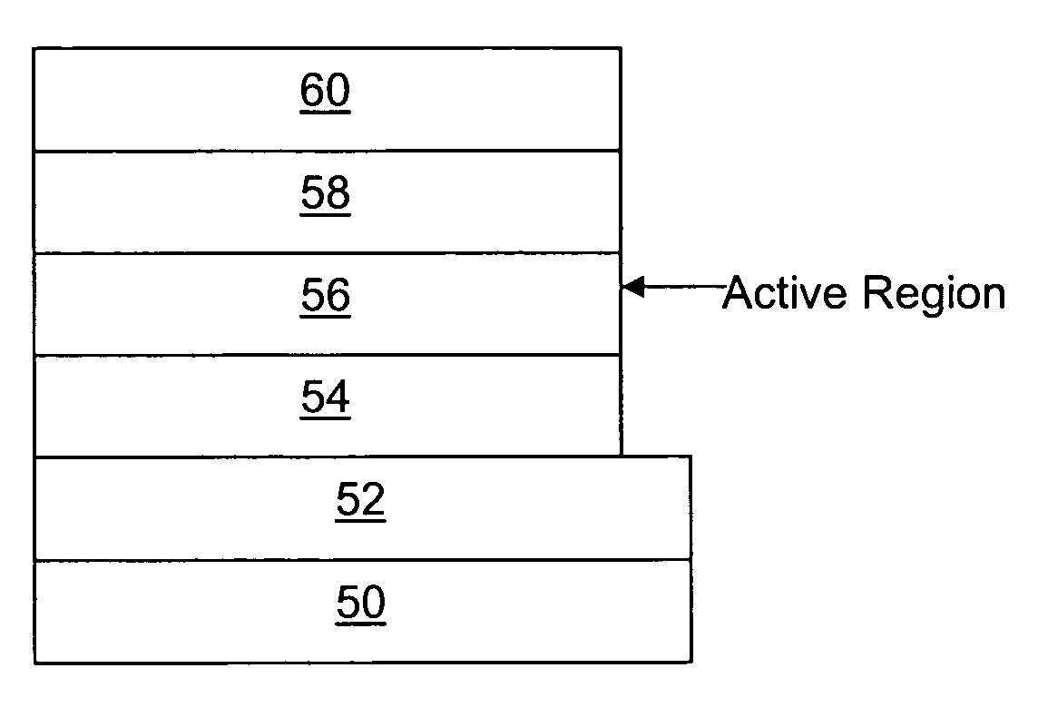
Zinc oxide crystal growth substrate
a technology of crystal growth substrate and zinc oxide, which is applied in the direction of polycrystalline material growth, natural mineral layered products, water-setting substance layered products, etc., can solve the problems of inferior device performance, sapphire and silicon carbide substrates are relatively expensive, and the optical properties are degraded
- Summary
- Abstract
- Description
- Claims
- Application Information
AI Technical Summary
Benefits of technology
Problems solved by technology
Method used
Image

Examples
example 1
Sputtering of ZnO
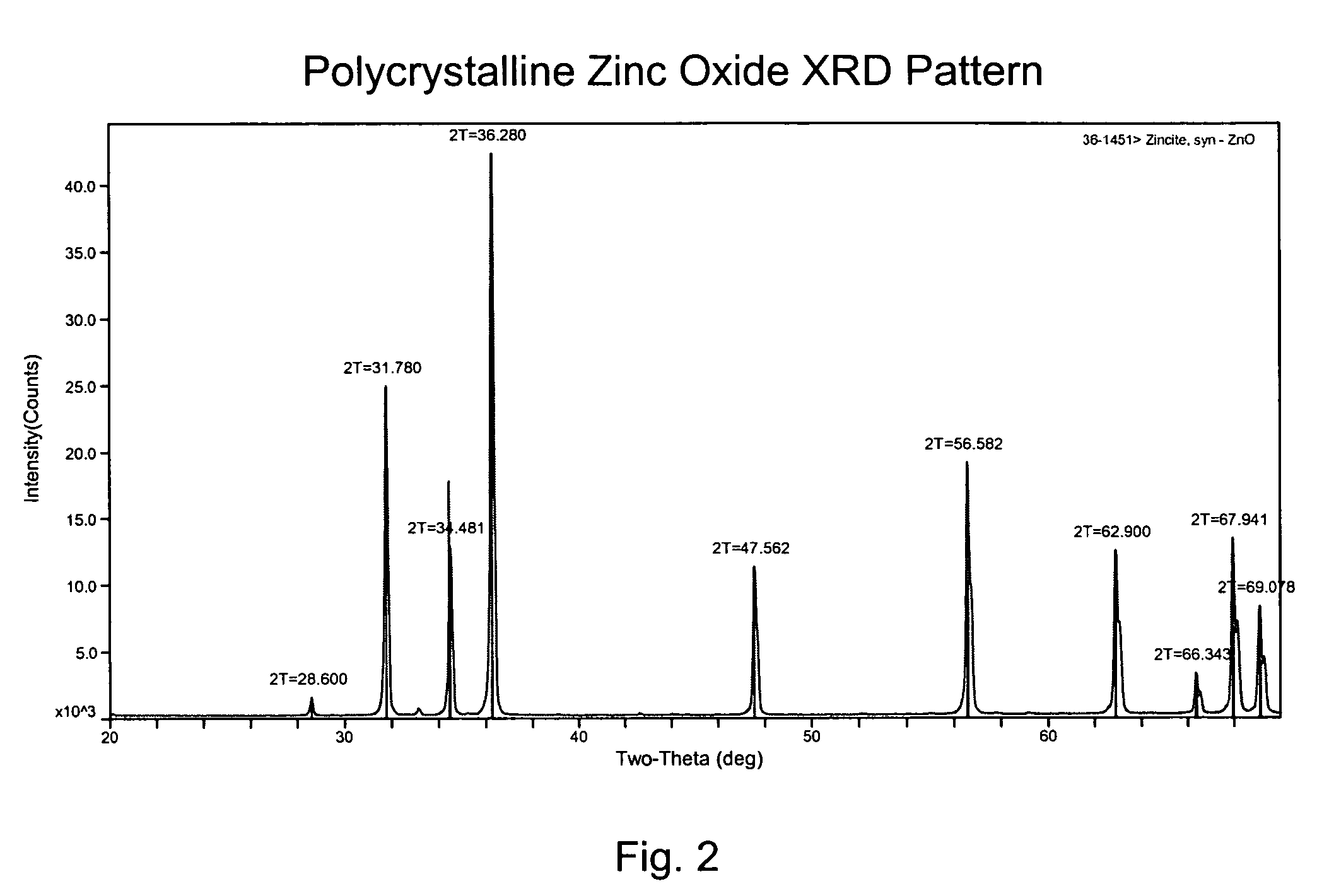
[0050]A thin film of undoped zinc oxide was deposited onto a self supporting substrate by RF sputtering. Both fused silica and silicon wafers were used as the self supporting substrate. The sputtering target composition was ZnO. The substrate temperature was between 350 and 550° C. The preferred temperature was about 400° C. The RF power was between 20 and 120 watts. The preferred power was about 60 watts. The sputtering atmosphere included argon at a gas pressure of about 4 to 20 mtorr and O2 at a gas pressure of about 1 to 4 mtorr. The preferred sputtering atmosphere pressures were about 9 mtorr argon and about 1 mtorr O2.
example 2
Sputtering of ZnO with Arsenic as a Dopant
[0051]A thin film of p-type zinc oxide was deposited onto a self supporting substrate by RF sputtering. Both fused silica and silicon wafers were used as the self supporting substrate. The sputtering target composition was ZnO (0.99–0.95 moles)+As (0.01–0.05 moles). The preferred target composition was ZnO (0.98 moles)+As (0.02 moles). The substrate temperature was between 350 and 550° C. The preferred temperature was about 400° C. The RF power was between 20 and 120 watts. The preferred power was about 60 watts. The sputtering atmosphere included argon at a gas pressure of about 4 to 20 mtorr and O2 at a gas pressure of about 1 to 4 mtorr. The preferred sputtering atmosphere pressures were about 9 mtorr argon and about 1 mtorr O2.
[0052]The resulting transparent p-type zinc oxide layer had a resistance of about 10,000 ohms / square. After annealing at 440° C. in air, the resistance dropped to about 1,000 ohms / square. In another composition pre...
example 3
Sputtering of ZnO with Arsenic as a Dopant
[0053]A thin film of p-type zinc oxide was deposited onto a self supporting substrate by RF sputtering. Both fused silica and silicon wafers were used as the self supporting substrate. The sputtering target composition was ZnO (0.99–0.95 moles)+As (0.01–0.05 moles). The preferred target composition was ZnO (0.98 moles)+As (0.02 moles). The substrate temperature was between 350 and 550° C. The preferred temperature was about 400° C. The RF power was between 20 and 120 watts. The preferred power was about 60 watts. The sputtering atmosphere included argon at a gas pressure of about 4 to 20 mtorr and H2 at a gas pressure of about 1 to 4 mtorr. The preferred sputtering atmosphere pressures were about 9 mtorr argon and about 1 mtorr H2.
[0054]The resulting transparent p-type zinc oxide layer had a resistance of about 500 ohms / square. Without being bound by theory, it is believed that the hydrogen gas may moderate the concentration of oxygen in the...
PUM
| Property | Measurement | Unit |
|---|---|---|
| thickness | aaaaa | aaaaa |
| power | aaaaa | aaaaa |
| RF frequency | aaaaa | aaaaa |
Abstract
Description
Claims
Application Information