Straight angle conductor and method of manufacturing the same

a technology of straight angle conductor and manufacturing method, which is applied in the direction of insulated conductors, flat/ribbon cables, and semiconductor/solid-state device details, etc. it can solve the problems of warping of lead wires, increased manufacturing costs, and insufficient soldering of wires with warping generated to silicon crystal wafers, so as to improve the flexibility of cladding materials and facilitate the generation of cutting-shear drop , the effect of preventing damage to silicon crystal wa

Active Publication Date: 2007-02-06
HITACHI METALS LTD
View PDF14 Cites 20 Cited by
  • Summary
  • Abstract
  • Description
  • Claims
  • Application Information

AI Technical Summary

Benefits of technology

[0012]An object of the present invention is to provide a straight angle conductor with a cladding material, which can improve performance of the straight angle conductor.
[0024]Further, one aspect of the present invention is to provide a straight angle conductor comprises a cladding material including a core-sheet metal and a conductor-sheet metal that sandwiches both surfaces of the core-sheet metal. An entirety or a part of an outer surface of the conductor-sheet metal is coated with a Sn—Pb solder layer or a Pb free solder layer. Accordingly when the straight angle conductor coated is used a lead wire for a solar cell, melting temperature in soldering the lead wire thereto is lowered to prevent damage of a silicon crystal wafer of the solar cell, as well as soldering areas are reduced to cut down on assembly costs.

Problems solved by technology

However, the lead frame described in Japanese Unexamined Patent Publication No. 2002-164560 is cut to form a circuit whereby a large amount of wasteful materials are produced, causing an increase of manufacturing costs.
When a lead wire, such as the lead frame described in Japanese Unexamined Patent Publication No. 2002-164560, using a straight angle conductor having a cladding material in the form of copper—INVER (registered trademark)—copper is corrected to be linear by applying tensile stress thereto so that the lead wire is more easily soldered to a contact area of the silicon crystal wafer, it tends to cause warping of the lead wire.
Therefore, there occurs the problem that the lead wire with the warping generated is not properly soldered to the silicon crystal wafer.

Method used


Image

  • Straight angle conductor and method of manufacturing the same
  • Straight angle conductor and method of manufacturing the same
  • Straight angle conductor and method of manufacturing the same

Examples


first embodiment

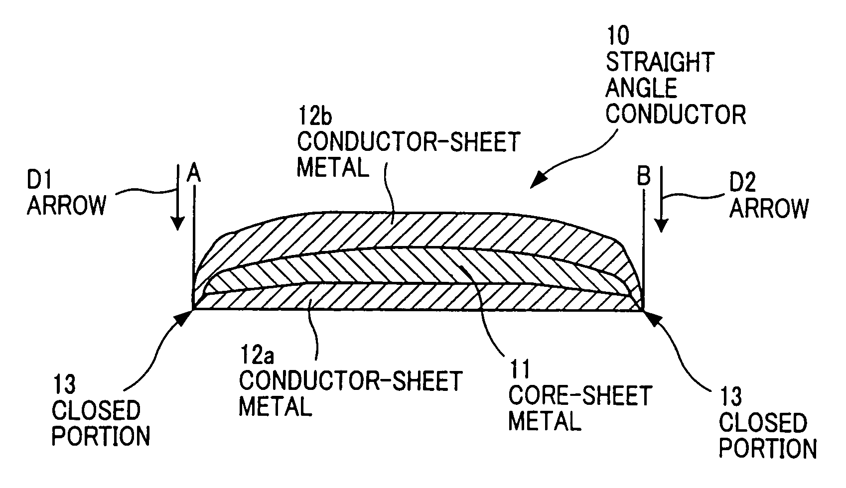
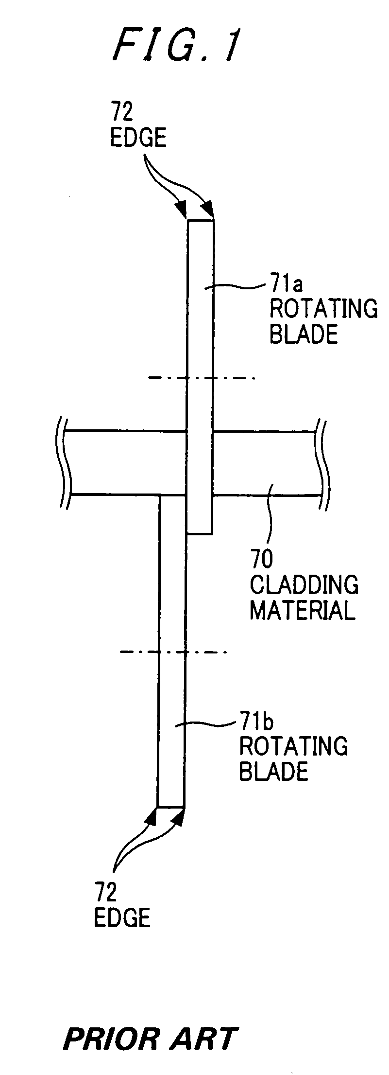
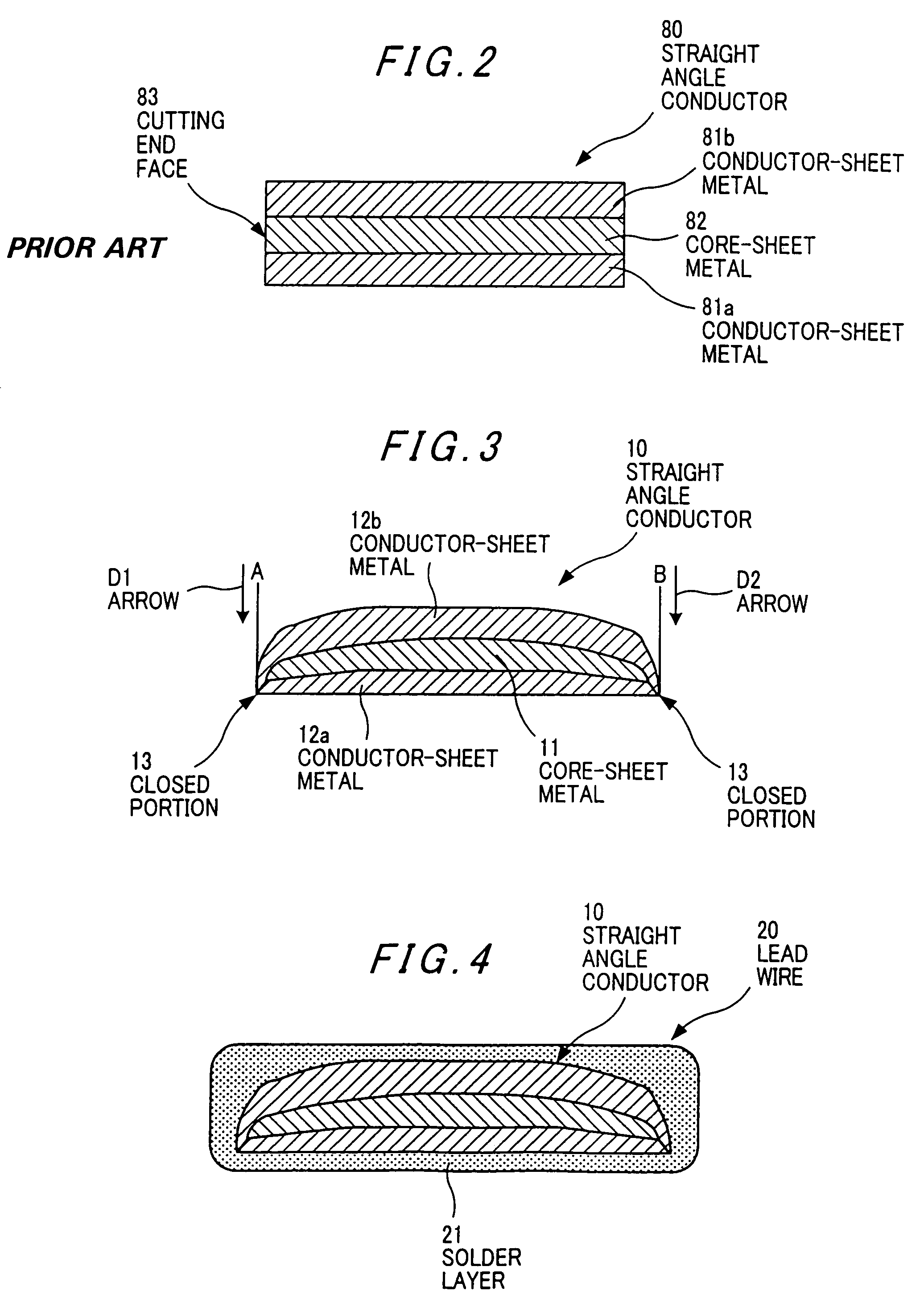
[0036]FIG. 2 shows a straight angle conductor 80 formed of a cladding material in the form of a copper material (conductor-sheet metal) 81a—an INVER (registered trademark) material (core-sheet metal) 82—a copper material (conductor-sheet metal) 81b with regard to the related art. This straight angle conductor 80 is produced by cutting the cladding material according to a slit method generally known as a cutting method with respect to metallic materials. In particular, as shown in FIG. 1, a cladding material 70 is cut successively in the direction perpendicular to the figure by using two sets of a pair of rotating blades 71a, 71b each of which is disposed above and under the cladding material 70 (only one set of a pair of blades shown in FIG. 1), to obtain the straight angle conductor 80 shown in FIG. 2.

[0037]Each edge 72 of the rotating blades 71a, 71b is finished in a sharp state or substantially vertical angle by grinding or the like. Each cutting end face (side end face) 83 of th...

second embodiment

[0074]FIG. 7 shows a transverse sectional view of a straight angle conductor of the preferred second embodiment according to the present invention.

[0075]As shown in FIG. 7, a straight angle conductor 50 according to the present embodiment includes a cladding material in which both faces of the core-sheet metal 51 having a thermal expansion coefficient equal to or less than 10 (×10−6 / C. °) are sandwiched by conductor-sheet metals 52a, 52b having a volume resistivity equal to or less than 5.0 (μΩ·cm).

[0076]And the conductor-sheet metals 52a, 52b have a random isotropic crystal orientation and an IR value shown in the following equation, which is equal to or sore than 0.15, preferably 0.20–0.70, particularly preferably 0.35–0.70.

IR=I(111) / {I(200)+I(111)}≧0.15.

[0077]Herein I (111): X ray diffraction intensity of Surface (111). I (200): X ray diffraction intensity of surface (200).

[0078]The core-sheet metal and the conductor-sheet metals which are similar to the core-sheet metal 11 and t...

third embodiment

[0091]A straight angle conductor of a third embodiment according to the present invention will be explained with reference to FIG. 3.

[0092]A basic construction of a straight angle conductor according to the present embodiment is the same as in the straight angle conductor 10 shown in FIG. 3, and the conductor-sheet metals 12a, 12b have further a random isotropic crystal orientation and an IR value shown in the following equation, which is equal to or more than 0.15, preferably 0.20–0.70, particularly preferably 0.35–0.70.

IR=I(111) / {I(200)+I(111)}≧0.15.

[0093]Herein I (111) X ray diffraction intensity of Surface (111). I (200): X ray diffraction intensity of Surface (200).

[0094]The straight angle conductor according to the present embodiment is manufactured by a method the same as the manufacturing method of the straight angle conductor 10 of the first embodiment described above.

[0095]The best mode of the straight angle conductor is formed by combining the core-sheet metal 11 made of ...


PUM

PropertyMeasurementUnit
volume resistivityaaaaaaaaaa
frequencyaaaaaaaaaa
thicknessaaaaaaaaaa

Abstract

A straight angle conductor 10 is provided with a cladding material including a core-sheet metal 11 and conductor-sheet metals 12a, 12b that sandwich both surfaces of the core-sheet metal 11. The conductor-sheet metals 12a, 12b having a volume resistivity equal to or less than 5.0 (μΩ·cm) wraps both sides of the core-sheet metal 11 having a thermal expansion coefficient equal to or less than 10 (×10−6 / C. °) to prevent the core-sheet metal 11 from being exposed to an outside of the conductor-sheet metals 12a, 12b. As a result, it prevents occurrence of an electrical potential difference in a boundary side face between the core-sheet metal 11 and the conductor-sheet metals 12a, 12b to improve corrosion resistance. Especially even when the straight angle conductor 10 is used on a silicon crystal wafer for a solar cell, damage of the silicon crystal wafer caused by heat occurring in soldering process of the conductor 10 or a change in temperature on use thereof for a solar cell is avoided.

Description

[0001]The present application is based on Japanese patent applications No. 2003-197242 and No. 2003-427591, the entire contents of which are incorporated herein by reference.BACKGROUND OF THE INVENTION[0002]1. Field of the Invention[0003]The present invention relates to a straight angle conductor and a method of manufacturing the same, and in particular to a straight angle conductor with a cladding material including a core-sheet material and a conductor-sheet material that sandwiches the core-sheet material.[0004]2. Description of the Related Art[0005]As a solar cell a semiconductor chip has been used in which silicon crystal wafer is grown on a substrate. A connection-lead wire is soldered to a predetermined area (contact area) of a silicon crystal wafer that results from cutting and dividing this semiconductor chip. The power is transmitted (outputted) through the connection-lead wire.[0006]A solder plated layer is usually formed on a surface of a conductor as a part of the conne...

Claims


Application Information

Patent Timeline
Patent Type & Authority Patents(United States)
IPC IPC(8): H02G3/06B23K35/26C22C13/00H01B1/02H01B5/02H01B13/00H01L23/48
CPCH01B1/026H01L2924/0002H01L2924/00Y02P80/30
Inventor ENDO, YUJUMATSUI, HAKARUAOYAMA, SEIGIICHIKAWA, TAKAAKI
Owner HITACHI METALS LTD
Why Eureka
Try Eureka